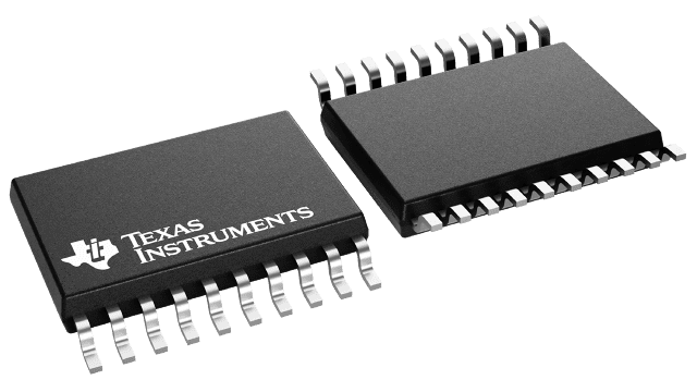
Gehäuseinformationen
| Gehäuse | Pins TSSOP (PW) | 20 |
| Betriebstemperaturbereich (°C) -40 to 125 |
| Gehäusemenge | Träger 2.000 | LARGE T&R |
Merkmale von SN74HCT244
- Operating voltage range of 4.5 V to 5.5 V
- High-current outputs drive up to 15 LSTTL loads
- Low power consumption: 80-µA maximum I CC
- Typical t pd = 13 ns
- ±6-mA output drive at 5 V
- Low input current of 1 µA maximum
- Inputs are TTL-voltage compatible
- 3-state outputs drive bus lines and buffer memory address registers
Beschreibung von SN74HCT244
These octal buffers and line drivers are designed specifically to improve both the performance and density of 3-state memory address drivers, clock drivers, and bus-oriented receivers and transmitters. The SNx4HCT244 devices are organized as two 4-bit buffers or drivers with separate output-enable ( OE) inputs. When OE is low, the device passes non inverted data from the A inputs to the Y outputs. When OE is high, the outputs are in the high-impedance state.
