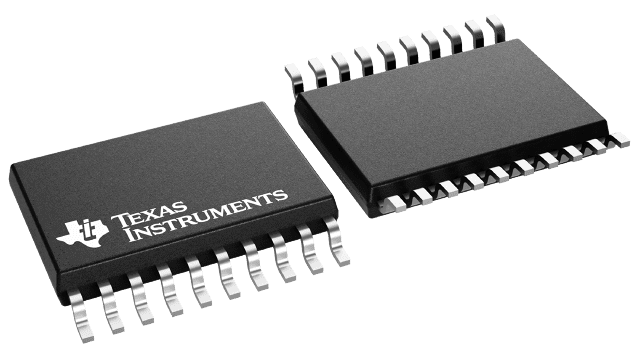
Gehäuseinformationen
| Gehäuse | Pins TSSOP (PW) | 20 |
| Betriebstemperaturbereich (°C) -40 to 125 |
| Gehäusemenge | Träger 70 | TUBE |
Merkmale von SN74LVC244A
- Operates From 1.65 V to 3.6 V
- Inputs Accept Voltages to 5.5 V
- Specified From –40°C to +85°C and –40°C to +125°C
- Maximum tpd of 5.9 ns at 3.3 V
- Typical VOLP (Output Ground Bounce) < 0.8 V at VCC = 3.3 V, TA = 25°C
- Typical VOHV (Output VOH Undershoot) > 2 V at VCC = 3.3 V, TA = 25°C
- Supports Mixed-Mode Signal Operation on All Ports (5-V Input or Output Voltage With 3.3-V VCC)
- Ioff Supports Live Insertion, Partial-Power-Down Mode, and Back-Drive Protection
- Can Be Used as a Down Translator to Translate Inputs From a Maximum of 5.5 V Down to the VCC Level
- Available in Ultra Small Logic QFN Package (0.5 mm Maximum Height)
- Latch-Up Performance Exceeds 250 mA Per JESD 17
- ESD Protection Exceeds JESD 22
- 2000-V Human-Body Model
- 1000-V Charged-Device Model
Beschreibung von SN74LVC244A
These octal bus buffers are designed for 1.65-V to 3.6-V VCC operation. The SN74LVC244A devices are designed for asynchronous communication between data buses.
