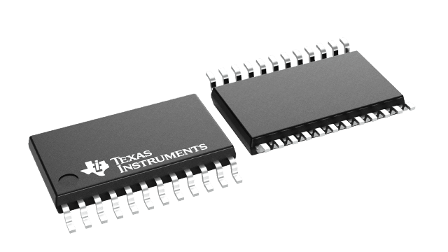
패키징 정보
| 패키지 | 핀 TSSOP (PW) | 24 |
| 작동 온도 범위(°C) -55 to 125 |
| 패키지 수량 | 캐리어 2,000 | LARGE T&R |
CD4067B의 주요 특징
- High-voltage types (20V rating)
- CD4067B – single 16-channel multiplexer or demultiplexer
- Low ON resistance: 125Ω (typ) over 15Vp-p signal-input range for VDD–VSS = 15V
- High OFF resistance: channel leakage of ±10pA (typ) at VDD – VSS = 10V
- Matched switch characteristics: RON = 5Ω (typ) for VDD – VSS = 15V
- Very low quiescent power dissipation under all digital-control input and supply conditions: 0.2µW (typ) at VDD – VSS = 10V
- Binary address decoding on chip
- 5V, 10V, and 15V parametric ratings
- 100% tested for quiescent current at 20V
- Standardized symmetrical output characteristics
- Maximum input current of 1µA at 18V over full package temperature range: 100nA at 18V and 25°C
- Meets all requirements of JEDEC tentative standard No. 13-B, Standard Specifications for Description of "B" Series CMOS Devices
CD4067B에 대한 설명
CD40x7B CMOS analog multiplexers or demultiplexers are digitally controlled analog switches having low ON impedance, low OFF leakage current, and internal address decoding. When these devices are used as demultiplexers, the channel in or out terminals are the outputs and the common out or in terminals are the inputs. In addition, the ON resistance is relatively constant over the full input-signal range.
The CD4067B is a 16-channel multiplexer with four binary control inputs, A, B, C, D, and an inhibit input, arranged so that any combination of the inputs selects one switch.
A logic "1" present at the inhibit input turns all channels off.
The CD40x7B types are supplied in 24-lead hermetic dual-in-line ceramic packages (F3A suffix), 24-lead dual-in-line plastic packages (E suffix), 24-lead small-outline packages (M, M96, and NSR suffixes), and 24-lead thin shrink small-outline packages (P and PWR suffixes).

