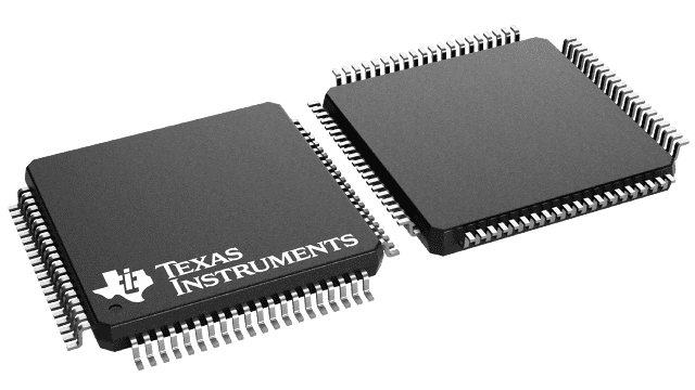
패키징 정보
| 패키지 | 핀 LQFP (PN) | 80 |
| 작동 온도 범위(°C) -40 to 85 |
| 패키지 수량 | 캐리어 119 | JEDEC TRAY (10+1) |
MSP430F5529의 주요 특징
- Low supply voltage range: 3.6 V down to 1.8 V
- Ultra-low power consumption
- Active mode (AM):
- All system clocks active:
- 290 µA/MHz at 8 MHz, 3.0 V, flash program execution (typical)
- 150 µA/MHz at 8 MHz, 3.0 V, RAM program execution (typical)
- All system clocks active:
- Standby mode (LPM3):
- Real-time clock (RTC) with crystal, watchdog, and supply supervisor operational, full RAM retention, fast wakeup:
- 1.9 µA at 2.2 V, 2.1 µA at 3.0 V (typical)
- Low-power oscillator (VLO), general-purpose counter, watchdog, and supply supervisor operational, full RAM retention, fast wakeup:
- 1.4 µA at 3.0 V (typical)
- Real-time clock (RTC) with crystal, watchdog, and supply supervisor operational, full RAM retention, fast wakeup:
- Off mode (LPM4):
- Full RAM retention, supply supervisor operational, fast wakeup:
- 1.1 µA at 3.0 V (typical)
- Full RAM retention, supply supervisor operational, fast wakeup:
- Shutdown mode (LPM4.5):
- 0.18 µA at 3.0 V (typical)
- Active mode (AM):
- Wake up from standby mode in 3.5 µs (typical)
- 16-bit RISC architecture, extended memory, up to 25-MHz system clock
- Flexible power-management system
- Fully integrated LDO with programmable regulated core supply voltage
- Supply voltage supervision, monitoring, and brownout
- Unified clock system
- FLL control loop for frequency stabilization
- Low-power low-frequency internal clock source (VLO)
- Low-frequency trimmed internal reference source (REFO)
- 32-kHz watch crystals (XT1)
- High-frequency crystals up to 32 MHz (XT2)
- 16-bit timer TA0, Timer_A with five capture/compare registers
- 16-bit timer TA1, Timer_A with three capture/compare registers
- 16-bit timer TA2, Timer_A with three capture/compare registers
- 16-bit timer TB0, Timer_B with seven capture/compare shadow registers
- Two universal serial communication interfaces (USCIs)
- USCI_A0 and USCI_A1 each support:
- Enhanced UART supports automatic baud-rate detection
- IrDA encoder and decoder
- Synchronous SPI
- USCI_B0 and USCI_B1 each support:
- I2C
- Synchronous SPI
- USCI_A0 and USCI_A1 each support:
- Full-speed universal serial bus (USB)
- Integrated USB-PHY
- Integrated 3.3-V and 1.8-V USB power system
- Integrated USB-PLL
- Eight input and eight output endpoints
- 12-bit analog-to-digital converter (ADC) (MSP430F552x only) with internal reference, sample-and-hold, and autoscan features
- Comparator
- Hardware multiplier supports 32-bit operations
- Serial onboard programming, no external programming voltage needed
- 3-channel internal DMA
- Basic timer with RTC feature
- Development tools and software (also see Tools and Software)
- LaunchPad™ development kit (MSP‑EXP430F5529LP)
- MSP430F5529 experimenter’s board (MSP‑EXP430F5529)
- 80-pin target development board (MSP‑TS430PN80USB)
- 64-pin target development board (MSP‑TS430RGC64USB)
- USB developers package (MSP430USBDEVPACK)
- MSP430Ware™ code examples
- Device Comparison summarizes the available family members
MSP430F5529에 대한 설명
The Texas Instruments MSP430F55xx microcontrollers (MCUs) are part of the MSP430™ system control & communication family of ultra-low-power microcontrollers consists of several devices featuring peripheral sets targeted for a variety of applications. The architecture, combined with extensive low-power modes, is optimized to achieve extended battery life in portable measurement applications. The microcontroller features a powerful 16-bit RISC CPU, 16-bit registers, and constant generators that contribute to maximum code efficiency. The digitally controlled oscillator (DCO) allows the devices to wake up from low-power modes to active mode in 3.5 µs (typical).
The MSP430F5529, MSP430F5527, MSP430F5525, and MSP430F5521 microcontrollers have integrated USB and PHY supporting USB 2.0, four 16-bit timers, a high-performance 12-bit analog-to-digital converter (ADC), two USCIs, a hardware multiplier, DMA, an RTC module with alarm capabilities, and 63 I/O pins. The MSP430F5528, MSP430F5526, MSP430F5524, and MSP430F5522 microcontrollers include all of these peripherals but have 47 I/O pins.
The MSP430F5519, MSP430F5517, and MSP430F5515 microcontrollers have integrated USB and PHY supporting USB 2.0, four 16-bit timers, two USCIs, a hardware multiplier, DMA, an RTC module with alarm capabilities, and 63 I/O pins. The MSP430F5514 and MSP430FF5513 microcontrollers include all of these peripherals but have 47 I/O pins.
Typical applications include analog and digital sensor systems, data loggers, and others that require connectivity to various USB hosts.
The MSP430F55xx MCUs are supported by an extensive hardware and software ecosystem with reference designs and code examples to get your design started quickly. Development kits include the MSP430F5529 USB LaunchPad™ development kit and the MSP430F5529 experimenter’s board as well as the MSP-TS430PN80USB 80-pin target development board and the MSP-TS430RGC64USB 64-pin target development board. TI also provides free MSP430Ware™ software, which is available as a component of Code Composer Studio™ IDE desktop and cloud versions within TI Resource Explorer. The MSP430 MCUs are also supported by extensive online collateral, training, and online support through the TI E2E™ support forum.
For complete module descriptions, see the MSP430F5xx and MSP430F6xx Family User’s Guide.
