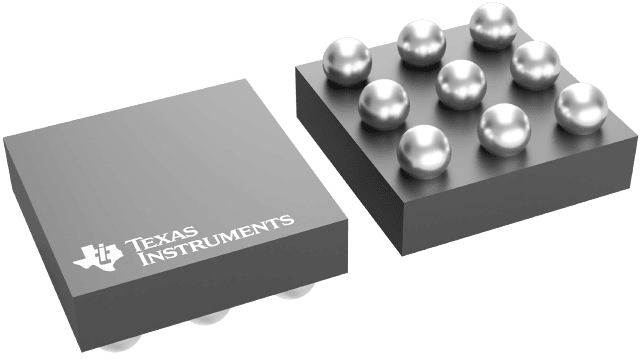
패키징 정보
| 패키지 | 핀 DSBGA (YZF) | 9 |
| 작동 온도 범위(°C) -40 to 85 |
| 패키지 수량 | 캐리어 3,000 | LARGE T&R |
TPA2034D1의 주요 특징
- Maximize Battery Life and Minimize Heat
- 0.5–µ Shutdown Current
- 3.0–mA Quiescent Current
- High Efficiency Class–D
- 88% at 400mW at 8

- 80% at 100mW at 8

- 88% at 400mW at 8
- Three Fixed Gain Versions
- TPA2032D1 has a gain of 2 V/V (6dB)
- TPA2033D1 has a gain of 3 V/V (9.5dB)
- TPA2034D1 has a gain of 4 V/V (12dB)
- Only One External Component Required
- Internal Matched Input Gain and Feedback Resistors for Excellent PSRR and CMRR
- Optimized PWM Output Stage Eliminates LC Output Filter
- PSRR (–75 dB) and Wide Supply Voltage (2.5 V to 5.5 V) Eliminates Need for a Dedicated Voltage Regulator
- Fully Differential Design Reduces RF Rectification and Eliminates Bypass Capacitor
- CMRR (–69 dB)Eliminates Two Input Coupling Capacitors
- Thermal and Short–Circuit Protection
- Pinout Very Similar to TPA2010D1
- Wafer Chip Scale Packaging (WCSP)
- NanoFree Lead–Free (Pb–Free: YZF)
- APPLICATIONS
- Ideal for Wireless Handsets, PDAs, and other mobile devices
TPA2034D1에 대한 설명
The TPA2032D1 (2V/V gain), TPA2033D1 (3V/V gain), and TPA2034D1 (4V/V gain) are 2.75–W high efficiency filter–free class–D audio power amplifiers, each in an approximately 1.5–mm × 1.5–mm wafer chip scale package (WCSP) that requires only one external component. The pinout is the same as the TPA2010D1 except that the external gain setting input resistors required by the TPA2010D1 are integrated into the fixed gain TPA203xD1 family.
Features like –75dB PSRR and improved RF–rectification immunity with a very small PCB footprint (WCSP amplifier plus single decoupling cap) make the TPA203xD1 family ideal for wireless handsets. A fast start–up time of 3.2 ms with minimal pop makes the TPA203xD1 family ideal for PDA applications.
In wireless handsets, the earpiece, speaker phone, and melody ringer can each be driven by a TPA203xD1. The TPA203xD1 family has a low 27–µV noise floor, A–weighted.
