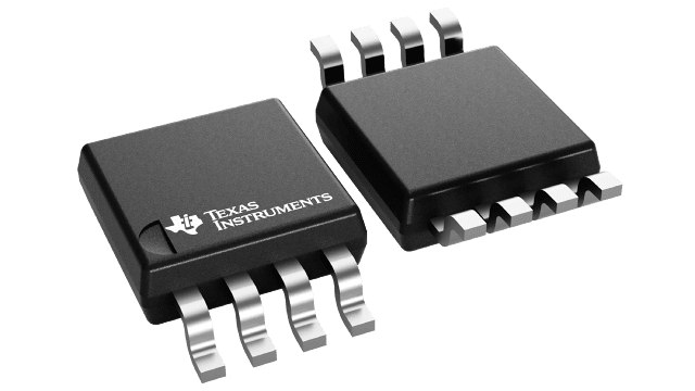
封裝資訊
| 封裝 | 針腳 VSSOP (DGK) | 8 |
| 操作溫度範圍 (°C) -40 to 125 |
| 包裝數量 | 運送業者 3,500 | LARGE T&R |
LMV762 的特色
- VS = 5 V, TA = 25°C, Typical Values Unless
Specified - Input Offset Voltage 0.2 mV
- Input Offset Voltage (Maximum Over Temp) 1 mV
- Input Bias Current 0.2 pA
- Propagation Delay (OD = 50 mV) 120 ns
- Low Supply Current 300 µA
- CMRR 100 dB
- PSRR 110 dB
- Extended Temperature Range −40°C to +125°C
- Push-Pull Output
- Ideal for 2.7-V and 5-V Single-Supply Applications
- Available in Space-Saving Packages:
- 6-Pin SOT-23 (Single With Shutdown)
- 8-Pin SOIC (Single With Shutdown)
- 8-Pin SOIC and VSSOP (Dual Without
Shutdown)
- LMV762Q-Q1 is Qualified for Automotive
Applications - AEC-Q100 Qualified With the Following Results:
- Device Temperature Grade 1: –40°C to
+125°C Ambient Operating Temperature
Range - Device HBM ESD Classification Level 1C
- Device CDM ESD Classification Level M2
- Device Temperature Grade 1: –40°C to
LMV762 的說明
The LMV76x devices are precision comparators intended for applications requiring low noise and low input offset voltage. The LMV761 single has a shutdown pin that can be used to disable the device and reduce the supply current. The LMV761 is available in a space-saving 6-pin SOT-23 or 8-Pin SOIC package. The LMV762 dual is available in 8-pin SOIC or VSSOP package. The LMV762Q-Q1 is available VSSOP and SOIC packages.
These devices feature a CMOS input and push-pull output stage. The push-pull output stage eliminates the need for an external pullup resistor.
The LMV76x are designed to meet the demands of small size, low power and high performance required by portable and battery-operated electronics.
The input offset voltage has a typical value of 200 µV at room temperature and a 1-mV limit over temperature.
