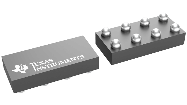
封裝資訊
| 封裝 | 針腳 DSBGA (YZP) | 8 |
| 操作溫度範圍 (°C) -40 to 85 |
| 包裝數量 | 運送業者 3,000 | LARGE T&R |
SN74LVC2G157 的特色
- Available in the Texas Instruments
NanoFree™ package - Supports 5-V VCC operation
- Inputs accept voltages to 5.5 V
- Max tpd of 6 ns at 3.3 V
- Low power consumption, 10-µA Maximum ICC
- ±24-mA Output drive at 3.3 V
- Typical VOLP (Output ground bounce)
<0.8 V at VCC = 3.3 V, TA = 25°C - Typical VOHV (Output VOH
undershoot)
>2 V at VCC = 3.3 V, TA = 25°C - Ioff Supports live insertion, partial-power-down mode, and back-drive protection
- Can be used as a down translator to translate inputs from a maximum of 5.5 V
down
to the VCC Level - Latch-up performance exceeds 100 mA per
JESD 78, Class II - ESD Protection exceeds JESD 22
- 2000-V Human body model (A114-A)
- 1000-V Charged-device model (C101)
SN74LVC2G157 的說明
This single 2-line to 1-line data selector multiplexer is designed for 1.65-V to 5.5-V VCC operation.
The SN74LVC2G157 device features a common strobe (G) input. When the strobe is high, Y is low and Y is high. When the strobe is low, a single bit is selected from one of two sources and is routed to the outputs. The device provides true and complementary data.
NanoFree™ package technology is a major breakthrough in IC packaging concepts, using the die as the package.
This device is fully specified for partial-power-down applications using Ioff. The Ioff circuitry disables the outputs, preventing damaging current backflow through the device when it is powered down.

