SLUAAH6 November 2021 LM5110 , LM5111 , LM5112 , LM5112-Q1 , LM5114 , LM5134 , LMG1020 , LMG1025-Q1 , SM74101 , TPS2811 , TPS2813 , TPS2818-EP , TPS2819-EP , TPS2828 , TPS2829 , UCC27321 , UCC27322 , UCC27322-EP , UCC27322-Q1 , UCC27323 , UCC27324 , UCC27325 , UCC27332-Q1 , UCC27423 , UCC27423-Q1 , UCC27424 , UCC27424-EP , UCC27424-Q1 , UCC27425 , UCC27444 , UCC27444-Q1 , UCC27511 , UCC27511A , UCC27511A-Q1 , UCC27512 , UCC27512-EP , UCC27516 , UCC27517 , UCC27517A , UCC27517A-Q1 , UCC27518 , UCC27518A-Q1 , UCC27519 , UCC27519A-Q1 , UCC27523 , UCC27524 , UCC27524A , UCC27524A-Q1 , UCC27524A1-Q1 , UCC27525 , UCC27526 , UCC27527 , UCC27528 , UCC27531 , UCC27531-Q1 , UCC27532 , UCC27532-Q1 , UCC27533 , UCC27536 , UCC27537 , UCC27538 , UCC27611 , UCC27614 , UCC27614-Q1 , UCC27624 , UCC27624-Q1 , UCC37321 , UCC37322 , UCC37323 , UCC37324 , UCC37325 , UCC44273 , UCC57102 , UCC57102-Q1 , UCC57108 , UCC57108-Q1
1 Density
Modern power converter modules pack high power in a very small size. For example, power brick modules, such as 1/4 brick packs, supply in excess of 800W, eight brick packs in excess of 600W, and sixteen brick can pack more than 400W. Electronic components, such as gate drivers, need to match the trend of increased power density by offering small package sizes. A comparison of solutions sizes is shown in Table 1-1.
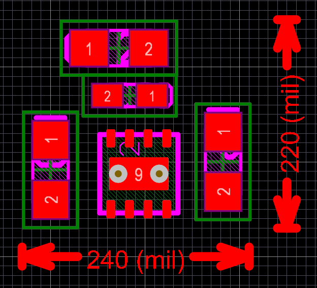
The UCC27614 gate driver helps minimize PCB area in the gate drive section of the board by using a smaller package (2mm x 2mm) while accomplishing the same or higher drive current (10-A) capability than most commonly available dual channel low-side gate drivers. Gate drivers are typically used in applications that require multiple MOSFETs to be driven, such as synchronous rectifiers. The solution size of using two UCC27614 is smaller than a single IC, dual channel solution. This solution size advantage allows designers to have increased drive strength, use less space, and optimize PCB layout.
 Figure 1-1 Layout Example of UCC27614
(2mm x 2mm)
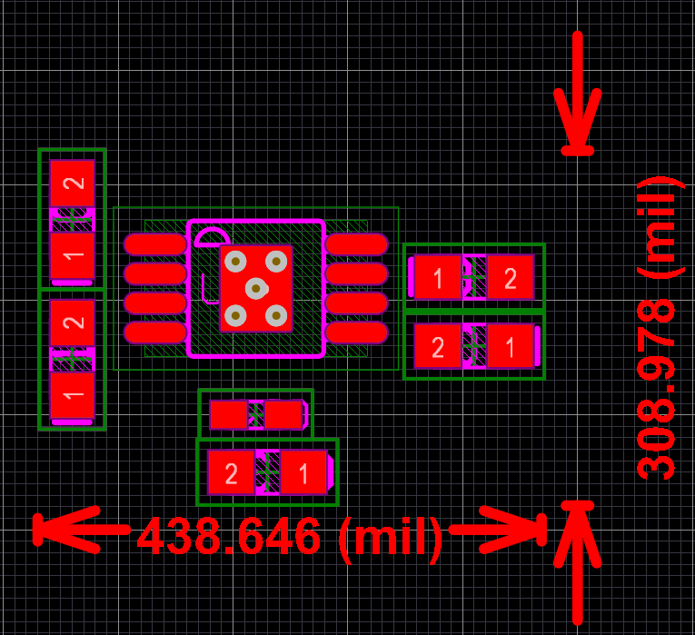
  Figure 1-2 Layout Example of MSOP
(5mm x 3mm) Driver
Figure 1-2 Layout Example of MSOP
(5mm x 3mm) DriverFigure 1-1 and Figure 1-2 shows a PCB area comparison between UCC27614 and a commonly available MSOP (5mm x 3mm) dual channel low-side driver using a simplified gate drive circuit with a single gate resistor and 2 decoupling capacitors. Since synchronous rectification requires 2 channels, the UCC27614 solution uses 2 IC’s for a total solution size of 68.13mm2 while the dual channel solution results in 87.44mm2. Total solution size is summarized in Table 1-1 where the 2 UCC27614 ICs results in 22.1% smaller solution size.
| UCC27614 | Dual Channel Low-Side Driver | |
|---|---|---|
| Total IC's | 2 | 1 |
| IC Package | 2mm x 2mm | 5mm x 3mm |
| Max Operating Voltage | 30 V | 26 V |
| Peak Pulsed Current | 10 A | 5 A |
| Solution Size | 2 x 6.1mm x 5.6mm | 1 x 11.1mm x 7.85mm |
| Total Solution Size | 68.32mm2 | 87.14mm2 |
The layout plays an important role in optimally driving the switching power device such as MOSFETs. When the gate driver is placed far from the MOSFET, the value of the parasitic elements, such as loop inductance, increases. This increased loop inductance causes high frequency noise. Due to this high frequency noise, the system might need additional snubber components or a larger EMI filter. In worst case, this high frequency noise might cause excess stress and damage on the components. Because of its small size, UCC27614 can be placed extremely close to the power MOSFETs and helps avoid most layout related issues.