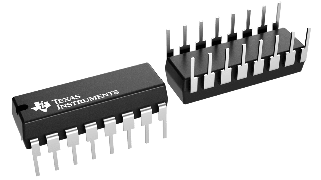
Gehäuseinformationen
| Gehäuse | Pins PDIP (N) | 16 |
| Betriebstemperaturbereich (°C) -55 to 125 |
| Gehäusemenge | Träger 25 | TUBE |
Merkmale von CD74ACT109
- Inputs Are TTL-Voltage Compatible
- Speed of Bipolar F, AS, and S, With Significantly Reduced Power Consumption
- Balanced Propagation Delays
- ±24-mA Output Drive Current
- Fanout to 15 F Devices
- SCR-Latchup-Resistant CMOS Process and Circuit Design
- Exceeds 2-kV ESD Protection Per MIL-STD-883, Method 3015
Beschreibung von CD74ACT109
The ’ACT109 devices contain two independent J-K\ positive-edge-triggered flip-flops. A low level at the preset (PRE)\ or clear (CLR)\ inputs sets or resets the outputs, regardless of the levels of the other inputs. When PRE\ and CLR\ are inactive (high), data at the J and K\ inputs meeting the setup-time requirements are transferred to the outputs on the positive-going edge of the clock (CLK) pulse. Clock triggering occurs at a voltage level and is not directly related to the rise time of the clock pulse. Following the hold-time interval, data at the J and K\ inputs can be changed without affecting the levels at the outputs. These versatile flip-flops can perform as toggle flip-flops by grounding K\ and tying J high. They also can perform as D-type flip-flops if J and K\ are tied together.
