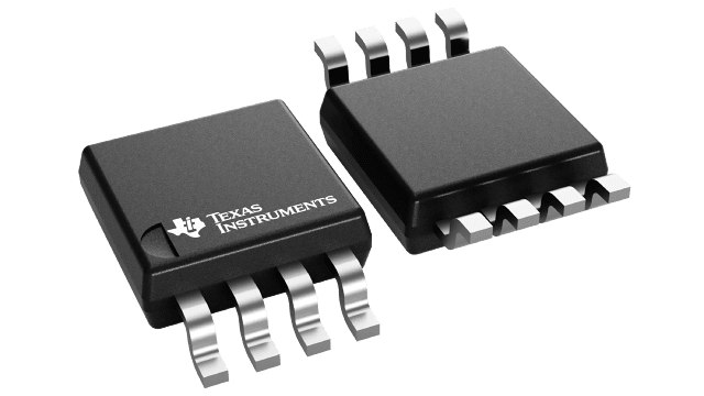
Gehäuseinformationen
| Gehäuse | Pins VSSOP (DGK) | 8 |
| Betriebstemperaturbereich (°C) -40 to 125 |
| Gehäusemenge | Träger 3.500 | LARGE T&R |
Merkmale von LMV842-Q1
- AEC-Q100 Automotive Qualification Test Guidance With the Following:
- Device Temperature Grade 1: –40°C to +125°C Ambient Operating Temperature
- Device HBM ESD Classification Level 2
- Device CDM ESD Classification Level C3
- Unless Otherwise Noted, Typical Values at
TA = 25 °C, V+ = 5 V. - Small 5-Pin SC70 Package (2.00 mm × 1.25 mm × 0.95 mm)
- Wide Supply Voltage Range: 2.7 V to 12 V
- Specified Performance at 3.3 V, 5 V and ±5 V
- Low Supply Current: 1 mA Per Channel
- Unity Gain Bandwidth: 4.5 MHz
- Open-Loop Gain: 133 dB
- Input Offset Voltage: 500 µV Maximum
- Input Bias Current: 0.3 pA
- CMRR at 112 dB and PSSR at 108 dB
- Input Voltage Noise: 20 nV/√Hz
- Temperature Range: −40°C to 125°C
- Rail-to-Rail Input and Output (RRIO)
Beschreibung von LMV842-Q1
The LMV84x-Q1 devices are low-voltage and low-power operational amplifiers that operate with supply voltages ranging from 2.7 V to 12 V and have rail-to-rail input and output capability. Their low offset voltage, low supply current, and CMOS inputs make them ideal for high impedance sensor interface and battery-powered applications.
The single LMV841-Q1 is offered in the space-saving 5-pin SC70 package, the dual LMV842-Q1 in the 8-pin VSSOP and 8-pin SOIC packages, and the quad LMV844-Q1 in the 14-pin TSSOP and 14-pin SOIC packages. These small packages are ideal solutions for area-constrained PCBs and portable electronics.
The LMV841-Q1, LMV842-Q1, and LMV844-Q1 incorporate enhanced manufacturing and support processes for the automotive market, including defect detection methodologies. Reliability qualification is compliant with the requirements and temperature grades defined in the AEC-Q100 standard.
