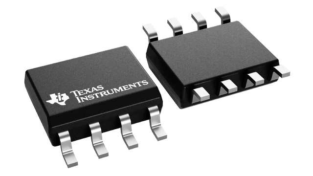
Gehäuseinformationen
| Gehäuse | Pins SOIC (D) | 8 |
| Betriebstemperaturbereich (°C) -40 to 85 |
| Gehäusemenge | Träger 2.500 | LARGE T&R |
Merkmale von LPC662
Rail-to-rail output swing |
|
Micropower operation (<0.5 mW) |
|
Specified for 100 k |
|
High voltage gain |
120 dB |
Low input offset voltage |
3 mV |
Low offset voltage drift |
1.3 µV/°C |
Ultra low input bias current |
2 fA |
Input common-mode includes GND |
|
Operating range from +5V to +15V |
|
Low distortion |
0.01% at 1 kHz |
Slew rate |
0.11 V/µs |
Full military temperature range available |
Beschreibung von LPC662
The LPC662 CMOS Dual operational amplifier is ideal for operation from a single supply. It features a wide range of operating voltage from +5V to +15V, rail-to-rail output swing in addition to an input common-mode range that includes ground. Performance limitations that have plagued CMOS amplifiers in the past are not a problem with this design. Input VOS, drift, and broadband noise as well as voltage gain (into 100 k![]() and 5 k
and 5 k![]() ) are all equal to or better than widely accepted bipolar equivalents, while the power supply requirement is typically less than 0.5 mW.
) are all equal to or better than widely accepted bipolar equivalents, while the power supply requirement is typically less than 0.5 mW.
This chip is built with National's advanced Double-Poly Silicon-Gate CMOS process.
See the LPC660 datasheet for a Quad CMOS operational amplifier and LPC661 for a single CMOS operational amplifier with these same features.
