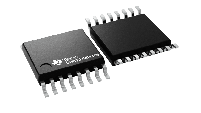
Información de empaque
| Encapsulado | Pines TSSOP (PW) | 16 |
| Rango de temperatura de funcionamiento (℃) -40 to 85 |
| Cant. de paquetes | Empresa de transporte 2,000 | LARGE T&R |
Características para DAC8802
- Relative Accuracy: 1 LSB Max
- Differential Nonlinearity: 1 LSB Max
- 2-mA Full-Scale Current ±20%, with VREF = ±10 V
- 0.5 µs Settling Time
- Midscale or Zero-Scale Reset
- Separate 4Q Multiplying Reference Inputs
- Reference Bandwidth: 10 MHz
- Reference Dynamics: -105 dB THD
- SPI™-Compatible 3-Wire Interface: 50 MHz
- Double Buffered Registers to Enable Simultaneous Multichannel Update
- Internal Power-On Reset
- Industry-Standard Pin Configuration
- APPLICATIONS
- Automatic Test Equipment
- Instrumentation
- Digitally Controlled Calibration
SPI is a trademark of Motorola, Inc.
All other trademarks are the property of their respective owners.
Descripción de DAC8802
The DAC8802 is a dual, 14-bit, current-output digital-to-analog converter (DAC) designed to operate from a single 2.7 V to 5.5 V supply.
The applied external reference input voltage VREF determines the full-scale output current. An internal feedback resistor (RFB) provides temperature tracking for the full-scale output when combined with an external I-to-V precision amplifier.
A doubled-buffered, serial data interface offers high-speed, 3-wire, SPI and microcontroller compatible inputs using serial data in (SDI), clock (CLK), and a chip-select (CS). A common level-sensitive load DAC strobe (LDAC) input allows simultaneous update of all DAC outputs from previously loaded input registers. Additionally, an internal power-on reset forces the output voltage to zero at system turn-on. An MSB pin allows system reset assertion (RS) to force all registers to zero code when MSB = 0, or to half-scale code when MSB = 1.
The DAC8802 is available in an TSSOP-16 package.
