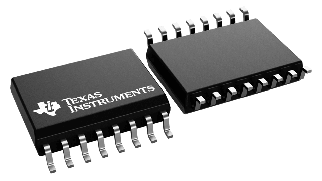
パッケージ情報
| パッケージ | ピン数 SOIC (DW) | 16 |
| 動作温度範囲 (℃) -40 to 125 |
| パッケージ数量 | キャリア 2,000 | LARGE T&R |
UCC21542 の特徴
- Wide body package options
- DW SOIC-16: pin-2-pin to UCC21520
- DWK SOIC-14: 3.3 mm Ch-2-Ch spacing
- Up to 4A peak source and 6A peak sink output
- Up to 18V VDD output drive supply
- 5V and 8V VDD UVLO options
- CMTI greater than 125V/ns
- Switching parameters:
- 33ns typical propagation delay
- 6ns maximum pulse-width distortion
- 10µs maximum VDD power-up delay
- Resistor-programmable dead time
- TTL and CMOS compatible inputs
- Safety-related
certifications
(planned):
- 8000VPK reinforced isolation per DIN EN IEC 60747-17 (VDE 0884-17)
- 5700VRMS isolation for 1 minute per UL 1577
- CQC certification per GB4943.1-2022
UCC21542 に関する概要
The UCC2154x is an isolated dual channel gate driver family designed with up to 4 A/6 A peak source/sink current to drive power MOSFET, IGBT, and GaN transistors. UCC2154x in DWK package also offers 3.3-mm minimum channel-to-channel spacing, which facilitates higher bus voltage.
The UCC2154x family can be configured as two low-side drivers, two high-side drivers, or a half-bridge driver. The input side is isolated from the two output drivers by a 5.7-kVRMS isolation barrier, with a minimum of 125-V/ns common-mode transient immunity (CMTI).
Protection features include: resistor programmable dead time, disable feature to shut down both outputs simultaneously, and negative voltage handling for up to –5-V spikes for 50 ns on input pins. All supplies have UVLO protection.
