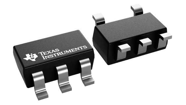
パッケージ情報
| パッケージ | ピン数 SOT-23 (DBV) | 5 |
| 動作温度範囲 (℃) -40 to 125 |
| パッケージ数量 | キャリア 3,000 | LARGE T&R |
UCC27517A-Q1 の特徴
- Qualified for Automotive Applications
- AEC-Q100 Qualified With the Following Results:
- Device Automotive Qualified Grade 1: –40°C
to 125°C Ambient Operating Temperature
Range - Device HBM ESD Classification Level 2
- Device CDM ESD Classification Level C6
- Device Automotive Qualified Grade 1: –40°C
- Low-Cost Gate-Driver Device Offering Superior
Replacement of NPN and PNP Discrete Solutions - 4-A Peak-Source and Sink Symmetrical Drive
- Ability to Handle Negative Voltages (–5 V) at
Inputs - Fast Propagation Delays (13-ns typical)
- Fast Rise and Fall Times (9-ns and 7-ns typical)
- 4.5 to 18-V Single-Supply Range
- Outputs Held Low During VDD UVLO (ensures
glitch-free operation at power up and power down) - TTL and CMOS Compatible Input-Logic Threshold
(independent of supply voltage) - Hysteretic-Logic Thresholds for High-Noise
Immunity - Dual Input Design (choice of an inverting (IN– pin)
or non-inverting (IN+ pin) driver configuration)- Unused Input Pin can be Used for Enable or
Disable Function
- Unused Input Pin can be Used for Enable or
- Output Held Low when Input Pins are Floating
- Input Pin Absolute Maximum Voltage Levels Not
Restricted by VDD Pin Bias Supply Voltage - Operating Temperature Range of –40°C to 140°C
- 5-Pin DBV (SOT-23) Package Option
UCC27517A-Q1 に関する概要
The UCC27517A-Q1 single-channel high-speed low-side gate-driver device effectively drives MOSFET and IGBT power switches. With a design that inherently minimizes shoot-through current, the UCC27517A-Q1 sources and sinks high peak-current pulses into capacitive loads offering rail-to-rail drive capability and extremely small propagation delay typically 13 ns.
The UCC27517A-Q1 device handles –5 V at input.
The UCC27517A-Q1 provides 4-A source and 4-A sink (symmetrical drive) peak-drive current capability at VDD = 12 V.
The UCC27517A-Q1 operates over a wide VDD range of 4.5 V to 18 V and wide temperature range of –40°C to 140°C. Internal Undervoltage Lockout (UVLO) circuitry on VDD pin holds the output low outside VDD operating range. The ability to operate at low voltage levels such as below 5 V, along with best-in-class switching characteristics, is especially suited for driving emerging wide band-gap power-switching devices such as GaN power-semiconductor devices.
