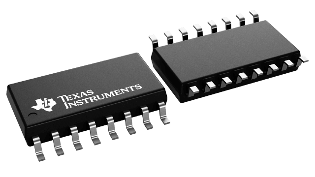
패키징 정보
| 패키지 | 핀 SOP (NS) | 16 |
| 작동 온도 범위(°C) -55 to 125 |
| 패키지 수량 | 캐리어 2,000 | LARGE T&R |
CD14538B의 주요 특징
- Retriggerable/resettable capability
- Trigger and reset propagation delays independent of RX, CX
- Triggering from leading or trailing edge
- Q and Q\ buffered outputs available
- Separate resets
- Replaces CD4538B Type
- Wide range of output-pulse widths
- Schmitt-trigger input allows unlimited rise and fall times on +TR and -TR inputs
- 100% tested for maximum quiescent current at 20 V
- Maximum input current of 1 µA at 18 V over full package-temperature range; 100 nA at 18 V and 25°C
- Noise margin (full package-temperature range):
- 1 V at VDD = 5 V
- 2 V at VDD = 10 V
- 2.5 V at VDD = 15 V
- 5-V, 10-V, and 15-V parametric ratings
- Standardized, symmetrical output characteristics
- Meets all requirements of JEDEC Tentative Standard No. 13B, "Standard Specifications for Description of 'B' Series CMOS Devices"
- Applications:
- Pulse delay and timing
- Pulse shaping
*T = 0.5 RXCX for CX  1000 pF
#T = RXCX; CXmin = 5000 pF
Data sheet acquired from Harris Semiconductor
CD14538B에 대한 설명
CD14538B dual precision monostable multivibrator provides stable retriggerable/resettable one-shot operation for any fixed-voltage timing application.
An external resistor (RX) and an external capacitor (CX) control the timing and accuracy for the circuit. Adjustment of RX and CX provides a wide range of output pulse widths from the Q and Q\ terminals. The time delay from trigger input to output transition (trigger propagation delay) and the time delay from reset input to output transition (reset propagation delay) are independent of RX and CX. Precision control of output pulse widths is achieved through linear CMOS techniques.
Leading-edge-triggering (+TR) and trailing-edge-triggering (-TR) inputs are provided for triggering from either edge of an input pulse. An unused +TR input should be tied to VSS. An unused -TR input should be tied to VDD. A RESET (on low level) is provided for immediate termination of the output pulse or to prevent output pulses when power is turned on. An unused RESET input should be tied to VDD. However, if an entire section of the CD14538B is not used, its inputs must be tied to either VDD or VSS. See Table 1.
In normal operation the circuit retriggers (extends the output pulse one period) on the application of each new trigger pulse. For operation in the non-retriggerable mode, Q\ is connected to -TR when leading-edge triggering (+TR) is used or Q is connected to +TR when trailing-edge triggering (-TR) is used. The time period (T) for this multivibrator can be calculated by: T = RXCX.
The minimum value of external resistance, RX, is 4 K . The minimum and maximum values of external capacitance, CX are 0 pF and 100µF, respectively.
The CD14538B is interchangeable with type MC14538 and is similar to and pin-compatible with the CD4098B* and CD4538B. It can replace the CD4538B which type is not recommended for new designs.
The CD14538B types are supplied in 16-lead hermetic dual-in-line ceramic packages (F3A suffix), 16-lead dual-in-line plastic packages (E suffix), 16-lead small-outline packages (M, M96, MT, and NSR suffixes), and 16-lead thin shrink small-outline packages (PW and PWR suffixes).
