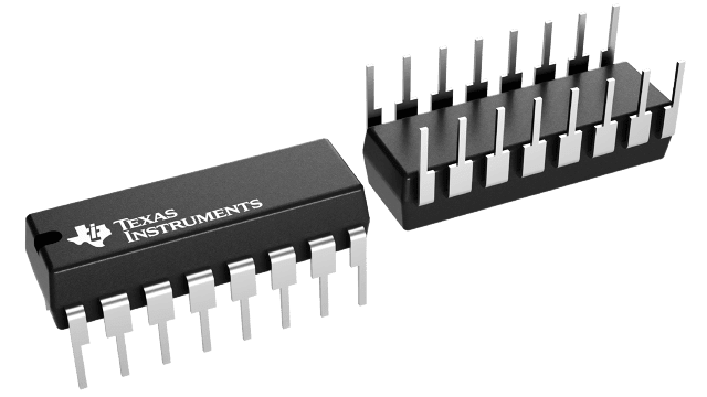
패키징 정보
| 패키지 | 핀 PDIP (N) | 16 |
| 작동 온도 범위(°C) -55 to 125 |
| 패키지 수량 | 캐리어 25 | TUBE |
CD40103B의 주요 특징
- Synchronous or asynchronous preset
- Medium-speed operation: fCL = 3.6 MHz (typ.) @ VDD = 10V
- Cascadable
- 100% tested for quiescent current at 20 V
- Maximum input current of 1 µA at 18 V over full package-temperature range; 100 nA at 18 V and 25°C
- Noise margin (full package-temperature range) =
1 V at VDD = 5 V
2 V at VDD = 10 V
2.5 V at VDD = 15 V - Standardized, symmetrical output characteristics
- 5-V, 10-V, and 15-V parametric ratings
- Meets all requirements of JEDEC Tentative Standard No. 13B, "Standard Specifications for Description of ’B’ Series CMOS Devices"
- Applications:
- Divide-by-"N" counters
- Programmable timers
- Interrupt timers
- Cycle/program counter
CD40102B - 2-Decade BCD Type
CD40103B - 8-Bit Binary Type
CD40103B에 대한 설명
CD40102B, and CD40103B consist of an 8-stage synchronous down counter with a single output which is active when the internal count is zero. The CD40102B is configured as two cascaded 4-bit BCD counters, and the CD40103B contains a single 8-bit binary counter. Each type has control inputs for enabling or disabling the clock, for clearing the counter to its maximum count, and for presetting the counter either synchronously or asynchronously. All control inputs and the CARRY-OUT/ZERO-DEFECT output are active-low logic.
In normal operation, the counter is decremented by one count on each positive transition of the CLOCK. Counting is inhibited when the CARRY-IN/COUNTER ENABLE (CI/CE)\ input is high. The CARRY-OUT/ZERO-DEFECT (CO/ZD)\ output goes low when the count reaches zero if the CI/CE\ input is low, and remains low for one full clock period.
When the SYNCHRONOUS PRESET-ENABLE (SPE)\ input is low, data at the JAM input is clocked input the counter on the next positive clock transition regardless of the state of the CI/CE\ input. When the ASYNCHRONOUS PRESET-ENABLE (APE)\ input is low, data at the JAM inputs is asynchronously forced into the counter regardless of the state of the SPE\, CI/CE\, or CLOCK inputs. JAM inputs JO-J7 represent two 4-bit BCD words for the CD40102B and a single 8-bit binary word for the CD40103B. When the CLEAR (CLR)\ input is low, the counter is asynchronously cleared to its maximum count (9910 for the CD40102B and 25510 for the CD40103B) regardless of the state of any other input. The precedence relationship between control inputs is indicated in the truth table.
If all control inputs except CI/CE\ are high at the time of zero count, the counters will jump to the maximum count, giving a counting sequence of 100 or 256 clock pulses long.
This causes the CO/ZD\ output to go low to enable the clock on each succeeding clock pulse.
The CD40102B and CD40103B may be cascaded using the CI/CE\ input and CO/ZD\ output, in either a synchronous or ripple mode as shown in Figs. 21 and 22.
The CD40102B and CD40103B types are supplied in 16-lead dual-in-line plastic packages (E suffix), 16-lead small-outline packages (NSR suffix), and 16-lead thin shrink small-outline packages (PW and PWR suffixes). The CD40103B types also are supplied in 16-lead hermetic dual-in-line ceramic packages (F3A suffix).
