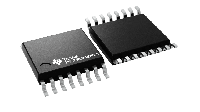
패키징 정보
| 패키지 | 핀 TSSOP (PW) | 16 |
| 작동 온도 범위(°C) -55 to 125 |
| 패키지 수량 | 캐리어 2,000 | LARGE T&R |
CD4052B의 주요 특징
- Wide range of digital and analog
signal levels:
- Digital: 3 V to 20 V
- Analog: ≤ 20 V P-P
- Low ON resistance, 125 Ω (typical) over 15 V P-P signal input range for V DD – V EE = 18 V
- High OFF resistance, channel leakage of ±100 pA (typical) at V DD – V EE = 18 V
- Logic-level conversion for digital addressing signals of 3 V to 20 V (V DD – V SS = 3 V to 20 V) to switch analog signals to 20 V P-P (V DD – V EE = 20 V) matched switch characteristics, r ON = 5 Ω (typical) for V DD – V EE = 15 V very low quiescent power dissipation under all digital-control input and supply conditions, 0.2 µW (typical) at V DD – V SS = V DD – V EE = 10 V
- Binary address decoding on chip
- 5 V, 10 V, and 15 V parametric ratings
- 100% tested for quiescent current at 20 V
- Maximum input current of 1 µA at 18 V over full package temperature range, 100 nA at 18 V and 25°C
- Break-before-make switching eliminates channel overlap
CD4052B에 대한 설명
The CD405xB analog multiplexers and demultiplexers are digitally-controlled analog switches having low ON impedance and very low OFF leakage current. These multiplexer circuits dissipate extremely low quiescent power over the full V DD – V SS and V DD – V EE supply-voltage ranges, independent of the logic state of the control signals.
