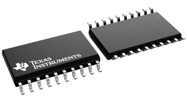
패키징 정보
| 패키지 | 핀 SOIC (DW) | 20 |
| 작동 온도 범위(°C) -40 to 85 |
| 패키지 수량 | 캐리어 2,000 | LARGE T&R |
SN74ABT573A의 주요 특징
- Typical VOLP (Output Ground Bounce)
<1 V at VCC = 5 V, TA = 25°C - High-Drive Outputs (–32-mA IOH, 64-mA IOL)
- Ioff Supports Partial-Power-Down Mode Operation
- Latch-Up Performance Exceeds 500 mA Per JEDEC Standard JESD 17
- ESD Protection Exceeds JESD 22
- 2000-V Human-Body Model (A114-A)
- 200-V Machine Model (A115-A)
SN74ABT573A에 대한 설명
These 8-bit latches feature 3-state outputs designed specifically for driving highly capacitive or relatively low-impedance loads. They are particularly suitable for implementing buffer registers, I/O ports, bidirectional bus drivers, and working registers.
The eight latches of the SN54ABT573 and SN74ABT573A are transparent D-type latches. While the latch-enable (LE) input is high, the Q outputs follow the data (D) inputs. When LE is taken low, the Q outputs are latched at the logic levels set up at the D inputs.
A buffered output-enable (OE)\ input can be used to place the eight outputs in either a normal logic state (high or low logic levels) or the high-impedance state. In the high-impedance state, the outputs neither load nor drive the bus lines significantly. The high-impedance state and increased drive provide the capability to drive bus lines without need for interface or pullup components.
OE\ does not affect the internal operations of the latches. Old data can be retained or new data can be entered while the outputs are in the high-impedance state.
To ensure the high-impedance state during power up or power down, OE\ should be tied to VCC through a pullup resistor; the minimum value of the resistor is determined by the current-sinking capability of the driver.
This device is fully specified for partial-power-down applications using Ioff. The Ioff circuitry disables the outputs, preventing damaging current backflow through the device when it is powered down.
