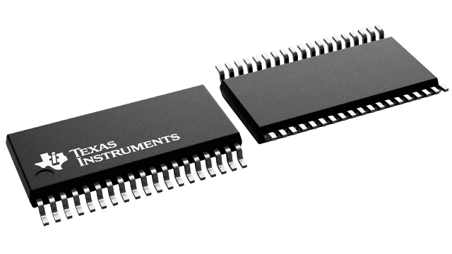
封裝資訊
| 封裝 | 針腳 TSSOP (DBT) | 38 |
| 操作溫度範圍 (°C) -40 to 105 |
| 包裝數量 | 運送業者 2,000 | LARGE T&R |
MSP430FR2355 的特色
- Embedded
microcontroller
- 16-bit RISC architecture up to 24 MHz
- Extended temperature: –40°C to 105°C
- Wide supply voltage range from 3.6 V down to 1.8 V (operational voltage is restricted by SVS levels, see VSVSH- and VSVSH+ in PMM, SVS and BOR)
- Optimized low-power
modes (at 3 V)
- Active mode: 142 µA/MHz
- Standby:
- LPM3 with 32768-Hz crystal: 1.43 µA (with SVS enabled)
- LPM3.5 with 32768-Hz crystal: 620 nA (with SVS enabled)
- Shutdown (LPM4.5): 42 nA (with SVS disabled)
- Low-power ferroelectric RAM
(FRAM)
- Up to 32KB of nonvolatile memory
- Built-in error correction code (ECC)
- Configurable write protection
- Unified memory of program, constants, and storage
- 1015 write cycle endurance
- Radiation resistant and nonmagnetic
- Ease of use
- 20KB ROM library includes driver libraries and FFT libraries
- High-performance analog
- One 12-channel 12-bit analog-to-digital converter (ADC)
- Internal shared reference (1.5, 2.0, or 2.5 V)
- Sample-and-hold 200 ksps
-
Two enhanced comparators (eCOMP)
- Integrated 6-bit digital-to-analog converter (DAC) as reference voltage
- Programmable hysteresis
- Configurable high-power and low-power modes
- One with fast 100-ns response time
- One with 1-µs response time with 1.5-µA low power
- Four smart analog combo (SAC-L3) (MSP430FR235x
devices only)
- Supports General-Purpose Operational Amplifier (OA)
- Rail-to-rail input and output
- Multiple input selections
- Configurable high-power and low-power modes
- Configurable PGA mode supports
- Noninverting mode: ×1, ×2, ×3, ×5, ×9, ×17, ×26, ×33
- Inverting mode: ×1, ×2, ×4, ×8, ×16, ×25, ×32
- Built-in 12-bit reference DAC for offset and bias settings
- 12-bit voltage DAC mode with optional references
- One 12-channel 12-bit analog-to-digital converter (ADC)
- Intelligent
digital peripherals
- Three 16-bit timers with three capture/compare registers each (Timer_B3)
- One 16-bit timer with seven capture/compare registers each (Timer_B7)
- One 16-bit counter-only real-time clock counter (RTC)
- 16-bit cyclic redundancy checker (CRC)
- Interrupt compare controller (ICC) enabling nested hardware interrupts
- 32-bit hardware multiplier (MPY32)
- Manchester codec (MFM)
- Enhanced serial
communications
- Two enhanced USCI_A (eUSCI_A) modules support UART, IrDA, and SPI
- Two enhanced USCI_B (eUSCI_B) modules support SPI and I2C
- Clock system
(CS)
- On-chip 32-kHz RC oscillator (REFO)
- On-chip 24-MHz
digitally controlled oscillator (DCO) with frequency locked loop (FLL)
- ±1% accuracy with on-chip reference at room temperature
- On-chip very low-frequency 10-kHz oscillator (VLO)
- On-chip high-frequency modulation oscillator (MODOSC)
- External 32-kHz crystal oscillator (LFXT)
- External high-frequency crystal oscillator up to 24 MHz (HFXT)
- Programmable MCLK prescaler of 1 to 128
- SMCLK derived from MCLK with programmable prescaler of 1, 2, 4, or 8
- General input/output and
pin functionality
- 44 I/Os on 48-pin package
- 32 interrupt pins (P1, P2, P3, and P4) can wake MCU from LPMs
- Development tools and software
(also see Tools and Software)
- LaunchPad™ development kit (MSP‑EXP430FR2355)
- Target development board (MSP‑TS43048PT)
- Free professional development environments
- Family members (also see
Device Comparison)
- MSP430FR2355: 32KB of program FRAM, 512 bytes of data FRAM, 4KB of RAM
- MSP430FR2353: 16KB of program FRAM, 512 bytes of data FRAM, 2KB of RAM
- MSP430FR2155: 32KB of program FRAM, 512 bytes of data FRAM, 4KB of RAM
- MSP430FR2153: 16KB of program FRAM, 512 bytes of data FRAM, 2KB of RAM
- Package options
- 48-pin: LQFP (PT)
- 40-pin: VQFN (RHA)
- 38-pin: TSSOP (DBT)
- 32-pin: VQFN (RSM)
MSP430FR2355 的說明
MSP430FR215x and MSP430FR235x microcontrollers (MCUs) are part of the MSP430™ MCU value line portfolio of ultra-low-power low-cost devices for sensing and measurement applications. MSP430FR235x MCUs integrate four configurable signal-chain modules called smart analog combos, each of which can be used as a 12-bit DAC or a configurable programmable-gain Op-Amp to meet the specific needs of a system while reducing the BOM and PCB size. The device also includes a 12-bit SAR ADC and two comparators. The MSP430FR215x and MSP430FR235x MCUs all support an extended temperature range from –40° up to 105°C, so higher temperature industrial applications can benefit from the devices’ FRAM data-logging capabilities. The extended temperature range allows developers to meet requirements of applications such as smoke detectors, sensor transmitters, and circuit breakers.
The MSP430FR215x and MSP430FR235x MCUs feature a powerful 16-bit RISC CPU, 16-bit registers, and a constant generator that contribute to maximum code efficiency. The digitally controlled oscillator (DCO) allows the device to wake up from low-power modes to active mode typically in less than 10 µs.
The MSP430 ultra-low-power (ULP) FRAM microcontroller platform combines uniquely embedded FRAM and a holistic ultra-low-power system architecture, allowing system designers to increase performance while lowering energy consumption. FRAM technology combines the low-energy fast writes, flexibility, and endurance of RAM with the nonvolatile behavior of flash.
MSP430FR215x and MSP430FR235x MCUs are supported by an extensive hardware and software ecosystem with reference designs and code examples to get your design started quickly. Development kits include the MSP-EXP430FR2355 LaunchPad™ development kit and the MSP-TS430PT48 48-pin target development board. TI also provides free MSP430Ware™ software, which is available as a component of Code Composer Studio™ IDE desktop and cloud versions within TI Resource Explorer. The MSP430 MCUs are also supported by extensive online collateral, training, and online support through the E2E™ support forums.
For complete module descriptions, see the MSP430FR4xx and MSP430FR2xx Family User’s Guide.

