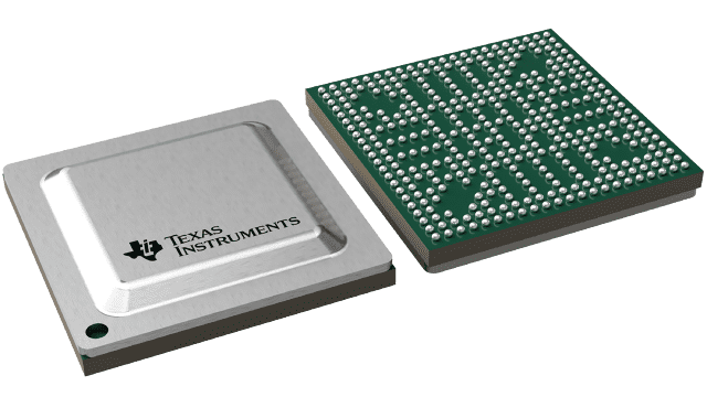
封裝資訊
| 封裝 | 針腳 FCBGA (ABF) | 367 |
| 操作溫度範圍 (°C) -40 to 125 |
| 包裝數量 | 運送業者 750 | LARGE T&R |
TDA3MV 的特色
- Architecture designed for ADAS applications
- Video and
image processing support
- Full-HD video (1920 × 1080p, 60 fps)
- Video input and video output
- Up to 2 C66x floating-point VLIW
DSP
- Fully object-code compatible with C67x and C64x+
- Up to thirty-two 16 × 16-bit fixed-point multiplies per cycle
- Up to 512kB of on-chip L3 RAM
- Level 3 (L3) and Level 4 (L4) interconnects
- Memory Interface (EMIF) module
- Supports DDR3/DDR3L up to DDR-1066
- Supports DDR2 up to DDR-800
- Supports LPDDR2 up to DDR-667
- Up to 2GB supported
- Dual Arm® Cortex®-M4 Image Processor Unit (IPU)
- Vision accelerationPac
- Embedded Vision Engine (EVE)
- Display
subsystem
- Display controller with DMA engine
- CVIDEO / SD-DAC TV analog composite output
- Video Input Port (VIP) module
- Support for up to 4 multiplexed input ports
- On-chip temperature sensor that is capable of generating temperature alerts
- General-Purpose Memory Controller (GPMC)
- Enhanced Direct Memory Access (EDMA) controller
- 3-port (2 external) Gigabit Ethernet (GMAC) switch
- Controller Area Network (DCAN) module
- CAN 2.0B protocol
- Modular Controller Area
Network (MCAN) module
- CAN 2.0B protocol
- Eight 32-bit general-purpose timers
- Three configurable UART modules
- Four Multichannel Serial Peripheral Interfaces (McSPI)
- Quad SPI interface
- Two Inter-Integrated Circuit (I2C™) ports
- Three Multichannel Audio Serial Port (McASP) modules
- Secure Digital Input Output Interface (SDIO)
- Up to 126 General-Purpose I/O (GPIO) pins
- Power, reset, and clock management
- On-chip debug with CTools technology
- Automotive AEC-Q100 qualified
- 15 × 15 mm, 0.65-mm pitch, 367-pin PBGA (ABF)
- Seven Dual Clock Comparators (DCC)
- Memory Cyclic Redundancy Check (CRC)
- TESOC (LBIST/PBIST) that enables field testing of logic and on-chip memory
- Error Signaling Module (ESM)
- Five instances of Real-Time Interrupt (RTI) modules that can be used as watch dog timers
- 8-channel 10-bit ADC
- MIPI® Camera Serial Interface 2 (CSI-2)
- PWMSS
- Full HW image pipe: DPC, CFA, 3D-NF,
RGB-YUV
- WDR, HW LDC and perspective
TDA3MV 的說明
TI’s TDA3x System-on-Chip (SoC) is a highly optimized and scalable family of devices designed to meet the requirements of leading Advanced Driver Assistance Systems (ADAS). The TDA3x family enables broad ADAS applications in automobiles by integrating an optimal mix of performance, low power, smaller form factor and ADAS vision analytics processing that aims to facilitate a more autonomous and collision-free driving experience.
The TDA3x SoC enables sophisticated embedded vision technology in today’s automobile by enabling the industry’s broadest range of ADAS applications including front camera, rear camera, surround view, radar, and fusion on a single architecture.
The TDA3x SoC incorporates a heterogeneous, scalable architecture that includes a mix of Texas Instruments (TI)’s fixed and floating-point TMS320C66x digital signal processor (DSP) generation cores, Vision AccelerationPac (EVE), and dual-Cortex-M4 processors. The device allows low power profile in different package options (including Package-On-Package) to enable small form factor designs. TDA3x SoC also integrates a host of peripherals including multi-camera interfaces (both parallel and serial) for LVDS-based surround view systems, displays, CAN and GigB Ethernet AVB.
The Vision AccelerationPac for this family of products includes embedded vision engine (EVE) offloading the vision analytics functionality from the application processor while also reducing the power footprint. The Vision AccelerationPac is optimized for vision processing with a 32-bit RISC core for efficient program execution and a vector coprocessor for specialized vision processing.
Additionally, TI provides a complete set of development tools for the Arm, DSP, and EVE coprocessor, including C compilers, a DSP assembly optimizer to simplify programming and scheduling, and a debugging interface for visibility into source code execution.
The TDA3x ADAS processor is qualified according to AEC-Q100 standard.