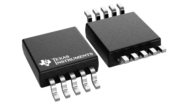
Gehäuseinformationen
| Gehäuse | Pins VSSOP (DGS) | 10 |
| Betriebstemperaturbereich (°C) -40 to 85 |
| Gehäusemenge | Träger 1.000 | SMALL T&R |
Merkmale von LMV712-N
- Available In Automotive AEC-Q100 Grade 1 Version (LMV712-N Only)
- 5-MHz GBP
- Slew Rate: 5 V/µs
- Low Noise: 20 nV/√Hz
- Supply Current: 1.22 mA/Channel
- VOS< 3 mV Maximum
- Ensured 2.7-V and 5-V Specifications
- Temperature Range: –40°C to 125°C
- Rail-to-Rail Inputs and Outputs
- Unity Gain Stable
- Small Package: 10-Pin DSBGA, 10-Pin WSON, and 10-Pin VSSOP
- 1.5-µA Shutdown ICC
- 2.2-µs Turnon
Beschreibung von LMV712-N
The LMV712-N devices are high-performance BiCMOS operational amplifiers intended for applications requiring rail-to-rail inputs combined with speed and low noise. They offer a bandwidth of 5 MHz and a slew rate of 5 V/µs, and can handle capacitive loads of up to 200 pF without oscillation.
The LMV712-N is ensured to operate from 2.7 V to 5.5 V and offers two independent shutdown pins. This feature allows disabling of each device separately and reduces the supply current to less than 1 µA typical. The output voltage rapidly ramps up smoothly with no glitch as the amplifier comes out of the shutdown mode.
The LMV712-N with the shutdown feature is offered in space-saving 10-pin DSBGA and 10-pin WSON packages. It is also offered in 10-pin VSSOP package. These packages are designed to meet the demands of small size, low power, and low cost required by cellular phones and similar battery-operated portable electronics.
