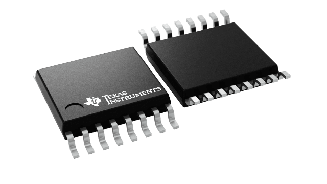
패키징 정보
| 패키지 | 핀 TSSOP (PW) | 16 |
| 작동 온도 범위(°C) -55 to 125 |
| 패키지 수량 | 캐리어 2,000 | LARGE T&R |
CD4572UB의 주요 특징
- Pin 7 NOR input positioned adjacent to VSS for easy use of gate as an inverter
- Pin 15 NAND input positioned adjacent to VDD for easy use of gate as an inverter
- Standard symmetrical output characteristics
- 100% tested for quiescent current at 20 V
- Maximum input current of 1 µA at 18 V over full package-temperature range:
100 nA at 18 V and 25°C - 5-V, 10-V, and 15-V parametric ratings
- Meets all requirements of JEDEC Tentative Standard No. 13B, "Standard Specifications for Description of 'B' Series CMOS Devices"
CD4572UB에 대한 설명
CD4572UB Hex Gate provides the system designer with direct implementation of inverter, NAND, and NOR functions and supplements the existing family of CMOS gates.
The CD4572UB devices meet all requirements of JEDEC Standard No. 13B, "Standard Specifications for Description of 'B' Series CMOS Devices."
The CD4572UB types are supplied in 16-lead dual-in-line plastic packages (E suffix), 16-lead small-outline packages (M, M96, MT, and NSR suffixes), and 16-lead thin shrink small-outline packages (PW and PWR suffixes).
