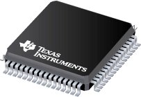
封裝資訊
| 封裝 | 針腳 VSSOP (DGS) | 28 |
| 操作溫度範圍 (°C) -40 to 125 |
| 包裝數量 | 運送業者 5,000 | LARGE T&R |
MSPM0G3507-Q1 的特色
- Core
- Arm 32-bit Cortex-M0+ CPU with memory protection unit, frequency up to 80MHz
-
Functional Safety Quality-Managed
- Functional Safety Manual and FMEDA available to aid in functional safety system design
- Operating characteristics
- Extended temperature: –40°C up to 125°C
- Wide supply voltage range: 1.62V to 3.6V
- Memories
- Up to 128KB of flash memory with error correction code (ECC)
- Up to 32KB of SRAM with hardware parity
- High-performance analog peripherals
- Two simultaneous sampling 12-bit 4Msps analog-to-digital converters (ADCs) with up to 17 external channels
- 14-bit effective resolution at 250ksps with hardware averaging
- One 12-bit 1Msps digital-to-analog converter with integrated output buffer (DAC)
- Two zero-drift zero-crossover chopper op-amps (OPA)
- 0.5µV/°C drift with chopping
- Integrated programmable gain stage, up to 32x
- One general-purpose amplifier (GPAMP)
- Three high-speed comparators (COMP) with 8-bit reference DACs
- 32ns propagation delay in high-speed mode
- Support low-power mode operation down to 0.7µA
- Programmable analog connections between ADC, OPAs, COMP and DAC
- Configurable 1.4V or 2.5V internal shared voltage reference (VREF)
- Integrated temperature sensor
- Integrated supply monitor
- Two simultaneous sampling 12-bit 4Msps analog-to-digital converters (ADCs) with up to 17 external channels
- Optimized low-power modes
- RUN: 101µA/MHz (CoreMark)
- SLEEP: 487µA at 4MHz
- STOP: 47µA at 32kHz
- STANDBY: 1.5µA with RTC and SRAM retention
- SHUTDOWN: 80nA with IO wake-up capability
- Intelligent digital peripherals
- 7-channel DMA controller
- Math accelerator supports DIV, SQRT, MAC and TRIG computations
- Seven timers supporting
up to 22 PWM channels
- One 16-bit general-purpose timer
- One 16-bit general-purpose timer supports QEI
- Two 16-bit general-purpose timers support low-power operation in STANDBY mode
- One 32-bit high-resolution general-purpose timer
- Two 16-bit advanced timers with deadband support up to 12 PWM channels
- Two window-watchdog timers
- RTC with alarm and calendar mode
- Enhanced communication interfaces
- Four UART interfaces; one supports LIN, IrDA, DALI, Smart Card, Manchester, and three support low-power operation in STANDBY mode
- Two I2C interfaces support up to FM+ (1Mbit/s), SMBus/PMBus, and wakeup from STOP mode
-
Two SPIs, one SPI supports up to 32Mbits/s
- One Controller Area Network (CAN) interface supports CAN 2.0 A or B and CAN-FD
- Clock system
- Internal 4MHz to 32MHz oscillator with up to ±1.2% accuracy (SYSOSC)
- Phase-locked loop (PLL) up to 80MHz
- Internal 32kHz low-frequency oscillator (LFOSC) with ±3% accuracy
- External 4MHz to 48MHz crystal oscillator (HFXT)
- External 32kHz crystal oscillator(LFXT)
- External clock input
- Data integrity and encryption
- Cyclic redundancy checker (CRC-16, CRC-32)
- True random number generator (TRNG)
- AES encryption with 128- or 256-bit key
- Flexible I/O features
- Up to 60 GPIOs
- Two 5V-tolerant IOs
- Two high-drive IOs with 20mA drive strength
- Up to 60 GPIOs
- Development support
- 2-pin serial wire debug (SWD)
- Package options
- 64-pin LQFP
- 48-pin LQFP, VQFN
- 32-pin VQFN
- 32 and 28-pin VSSOP
- Family members (also see Device Comparison)
- MSPM0G3505: 32KB flash, 16KB RAM
- MSPM0G3506: 64KB flash, 32KB RAM
- MSPM0G3507: 128KB flash, 32KB RAM
- Development kits and software (also see Tools and Software)
- LP-MSPM0G3507 LaunchPad™ development kit
- MSP Software Development Kit (SDK)
- Automotive qualification
- AEC-Q100 Grade 1
- 32- and 48-pin QFN with wettable flanks option
MSPM0G3507-Q1 的說明
MSPM0G350x microcontrollers (MCUs) are part of the MSP highly integrated, ultra-low-power 32-bit MCU family based on the enhanced Arm Cortex-M0+ 32-bit core platform operating at up to 80MHz frequency. These cost-optimized MCUs offer high-performance analog peripheral integration, support extended temperature ranges from -40°C to 125°C, and operate with supply voltages ranging from 1.62V to 3.6V.
The MSPM0G350x devices provide up to 128KB embedded flash program memory with built-in error correction code (ECC) and up to 32KB SRAM with hardware parity option. These MCUs also incorporate a memory protection unit, 7-channel DMA, math accelerator, and a variety of high-performance analog peripherals such as two 12-bit 4-Msps ADCs, configurable internal shared voltage reference, one 12-bit 1-Msps DAC, three high speed comparators with built-in reference DACs, two zero-drift zero-crossover op-amps with programmable gain, and one general-purpose amplifier. These devices also offer intelligent digital peripherals such as two 16-bit advanced control timers, five general-purpose timers (with one 16-bit general-purpose timer for QEI interface, two 16-bit general-purpose timers for STANDBY mode, and one 32-bit general-purpose timer), two windowed-watchdog timers, and one RTC with alarm and calendar modes. These devices provide data integrity and encryption peripherals (AES, CRC, TRNG) and enhanced communication interfaces (four UART, two I2C, two SPI, and CAN 2.0/FD).
The TI MSPM0 family of low-power MCUs consists of devices with varying degrees of analog and digital integration that allow customers to find the MCU that meets project needs. The MSPM0 MCU platform combines the Arm Cortex-M0+ platform with a holistic ultra-low-power system architecture, allowing system designers to increase performance while reducing energy consumption.
MSPM0G350x MCUs are supported by an extensive hardware and software ecosystem with reference designs and code examples to get the design started quickly. Development kits available for purchase include a LaunchPad™ development kit. TI also provides a free MSP Software Development Kit (SDK), which is available as a component of Code Composer Studio™ IDE desktop and cloud version within the TI Resource Explorer. MSPM0 MCUs are also supported by extensive online collateral, training with MSP Academy, and online support through the TI E2E™ support forums.
For complete module descriptions, see the MSPM0 G-Series 80MHz Microcontrollers Technical Reference Manual.
