SCEA131 September 2023 TXB0101 , TXB0102 , TXB0104 , TXB0104-Q1 , TXB0106 , TXB0106-Q1 , TXB0108 , TXB0302 , TXB0304 , TXS0101 , TXS0101-Q1 , TXS0102 , TXS0102-Q1 , TXS0104E , TXS0104E-Q1 , TXS0108E , TXS0108E-Q1
1 Introduction
Auto-Sensing level shifters are named so because their input(s) and output(s), can be used in applications to perform the same functionality to send and receive signals. The I/Os are designed with weaker drive strength than devices from other level shifting families, to be easily overdriven by the hosts. This makes auto-direction devices a requirement for bidirectional interfaces such as I2C, MDIO, Quad-SPI, etc.
One-shots (OS) are named so because their outputs will create a single pulse of a set time period for each input trigger. The most common input trigger method is a rising or falling edge. These circuits are also often referred to as edge rate accelerators because they produce an increased output drive strength for a short time, resulting in faster output transition rates over a device that does not include these circuits.
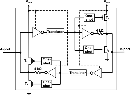
As part of the level shifter portfolio, TI offers TXS and TXB Level Shifter Families with one-shots. The one-shots are composed of a combination of logic with on-chip components. When the input of the device triggers, the one-shot circuit generates a pulse to the output MOSFET as shown in Table 1-1, bypassing the TXB's typical 4 kΩ output driver to produce a low-impedance output driver for a short time, improving the output's rise and fall time. This pulse width is a function of RC time constant and can also be impacted by additional or external RC components. It may also have variations with device-to-device or temperature.
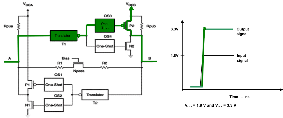
 Figure 1-1 Simplified One-Shot Circuitry
 Figure 1-3 TXS Architecture
 Figure 1-2 TXB Architecture
When the one-shot is triggered by an input, the output switches to an active state – on-state of the one-shot output for a set period of time and returns to its resting state – off-state, similar to Figure 3-13.
While the one-shot is active, the output resistance of the device is decreased. The low resistance path to VCCB through the pFET (P2) will cause the output to rise towards VCCB very quickly. Thereby, increasing the edge rate and maintaining DC drive for bidirectional I/Os.
After the one-shot expires, the internal pull-up of the TXS device drives the line high and maintains a steady state. The same is applicable with the internal buffer resistor of the TXB device.
Faster rising or falling input edges and the external load resistance and capacitance needs to be considered by ensuring < 70 pF to prevent damages to the device due to excessive current or power consumption. Section 3.3 and Table 1-1 further provides a general reference attributed to fast rising or falling inputs per lumped capacitance to avoid expiring the one-shot before the output reaches steady state. Similar to Implications of Slow or Floating CMOS Inputs, slower rising and falling inputs can also cause damage to the device due to excessive current / power consumption. For more guidelines using devices with one-shots, see Similar to Do's and Don'ts For TXS and TXB Voltage Level Shifters with Edge Rate Accelerators.
From using the standard 2.2 time constant, charge of ~86.5% transition times can be estimated (typically measured from 10% to 90%). Note that the typical pull-up resistance without the one-shot active is 10 kΩ and the typicall pull-up resistance with the one-shot active is 50 Ω. With typical load capacitance of 15 pF, the typical rise and fall times are compared below showing how the one-shots helps for faster rise/fall times. Section 2 further clarifies implications of slower rise/fall times for data throughput.
| Without one-shot | With one-shot | |
|---|---|---|
| Rise or Fall time (2.2×R×C) | 330 ns | 1.7 ns |