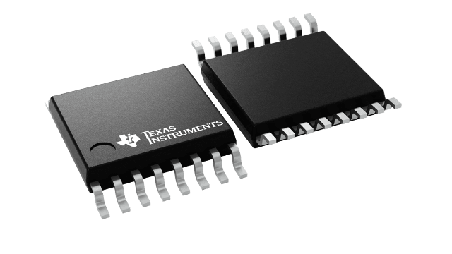
Información de empaque
| Encapsulado | Pines TSSOP (PW) | 16 |
| Rango de temperatura de funcionamiento (℃) -55 to 125 |
| Cant. de paquetes | Empresa de transporte 250 | SMALL T&R |
Características para CD74HC4050
- Typical Propagation Delay: 6ns at VCC = 5V, CL = 15pF, TA = 25°C
- High-to-Low Voltage Level Converter for up to VI = 16V
- Fanout (Over Temperature Range)
- Standard Outputs . . . . . . . . . . . . . . . 10 LSTTL Loads
- Bus Driver Outputs . . . . . . . . . . . . . 15 LSTTL Loads
- Wide Operating Temperature Range . . . –55°C to 125°C
- Balanced Propagation Delay and Transition Times
- Significant Power Reduction Compared to LSTTL Logic ICs
- HC Types
- 2V to 6V Operation
- High Noise Immunity: NIL = 30%, NIH = 30% of VCC at VCC = 5V
Descripción de CD74HC4050
The ’HC4049 and ’HC4050 are fabricated with high-speed silicon gate technology. They have a modified input protection structure that enables these parts to be used as logic level translators which convert high-level logic to a low-level logic while operating off the low-level logic supply. For example, 15-V input pulse levels can be down-converted to 0-V to 5-V logic levels. The modified input protection structure protects the input from negative electrostatic discharge. These parts also can be used as simple buffers or inverters without level translation. The ’HC4049 and ’HC4050 are enhanced versions of equivalent CMOS types.
