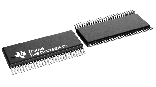
Información de empaque
| Encapsulado | Pines TVSOP (DGV) | 56 |
| Rango de temperatura de funcionamiento (℃) -40 to 85 |
| Cant. de paquetes | Empresa de transporte 2,000 | LARGE T&R |
Características para SN74LVCH16952A
- Member of the Texas Instruments Widebus™ Family
- Operates From 1.65 V to 3.6 V
- Inputs Accept Voltages to 5.5 V
- Max tpd of 6.6 ns at 3.3 V
- Typical VOLP (Output Ground Bounce)
<0.8 V at VCC = 3.3 V, TA = 25°C - Typical VOHV (Output VOH Undershoot)
>2 V at VCC = 3.3 V, TA = 25°C - Supports Mixed-Mode Signal Operation on All Ports (5-V Input/Output Voltage With 3.3-V VCC)
- Ioff Supports Partial-Power-Down Mode Operation
- Bus Hold on Data Inputs Eliminates the Need for External Pullup/Pulldown Resistors
- Latch-Up Performance Exceeds 250 mA Per JESD 17
- ESD Protection Exceeds JESD 22
- 2000-V Human-Body Model (A114-A)
- 200-V Machine Model (A115-A)
- 1000-V Charged-Device Model (C101)
Widebus is a trademark of Texas Instruments.
Descripción de SN74LVCH16952A
This 16-bit registered transceiver is designed for 1.65-V to 3.6-V VCC operation.
The SN74LVCH16952A contains two sets of D-type flip-flops for temporary storage of data flowing in either direction. The device can be used as two 8-bit transceivers or one 16-bit transceiver. Data on the A or B bus is stored in the registers on the low-to-high transition of the clock (CLKAB or CLKBA) input, provided that the clock-enable (CEAB\ or CEBA\) input is low. Taking the output-enable (OEAB\ or OEBA\) input low accesses the data on either port.
To ensure the high-impedance state during power up or power down, OE\ should be tied to VCC through a pullup resistor; the minimum value of the resistor is determined by the current-sinking capability of the driver.
Inputs can be driven from either 3.3-V or 5-V devices. This feature allows the use of these devices as translators in a mixed 3.3-V/5-V system environment.
This device is fully specified for partial-power-down applications using Ioff. The Ioff circuitry disables the outputs, preventing damaging current backflow through the device when it is powered down.
Active bus-hold circuitry holds unused or undriven inputs at a valid logic state. Use of pullup or pulldown resistors with the bus-hold circuitry is not recommended.
