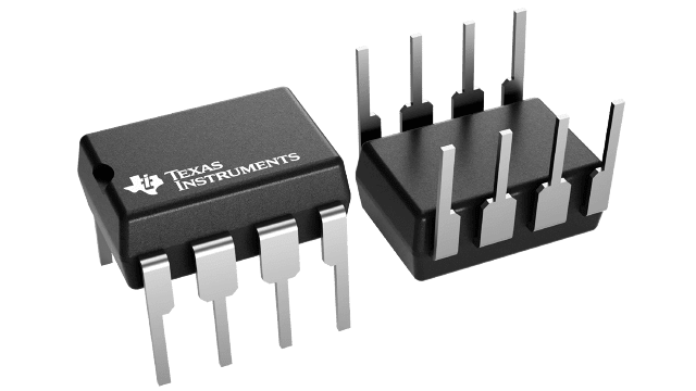
패키징 정보
| 패키지 | 핀 PDIP (P) | 8 |
| 작동 온도 범위(°C) 0 to 70 |
| 패키지 수량 | 캐리어 40 | TUBE |
LF356의 주요 특징
- Advantages
- Replace Expensive Hybrid and Module FET
Op Amps - Rugged JFETs Allow Blow-Out Free Handling
Compared With MOSFET Input Devices - Excellent for Low Noise Applications Using
Either High or Low Source Impedance–Very
Low 1/f Corner - Offset Adjust Does Not Degrade Drift or
Common-Mode Rejection as in Most
Monolithic Amplifiers - New Output Stage Allows Use of Large
Capacitive Loads (5,000 pF) Without Stability
Problems - Internal Compensation and Large Differential
Input Voltage Capability
- Replace Expensive Hybrid and Module FET
- Common Features
- Low Input Bias Current: 30 pA
- Low Input Offset Current: 3 pA
- High Input Impedance: 1012 Ω
- Low Input Noise Current: 0.01 pA/√Hz
- High Common-Mode Rejection Ratio: 100 dB
- Large DC Voltage Gain: 106 dB
- Uncommon Features
- Extremely Fast Settling Time to 0.01%:
- 4 µs for the LFx55 devices
- 1.5 µs for the LFx56
- 1.5 µs for the LFx57 (AV = 5)
- Fast Slew Rate:
- 5 V/µs for the LFx55
- 12 V/µs for the LFx56
- 50 V/µs for the LFx57 (AV = 5)
- Wide Gain Bandwidth:
- 2.5 MHz for the LFx55 devices
- 5 MHz for the LFx56
- 20 MHz for the LFx57 (AV = 5)
- Low Input Noise Voltage:
- 20 nV/√Hz for the LFx55
- 12 nV/√Hz for the LFx56
- 12 nV/√Hz for the LFx57 (AV = 5)
- Extremely Fast Settling Time to 0.01%:
LF356에 대한 설명
The LFx5x devices are the first monolithic JFET input operational amplifiers to incorporate well-matched, high-voltage JFETs on the same chip with standard bipolar transistors (BI-FET™ Technology). These amplifiers feature low input bias and offset currents/low offset voltage and offset voltage drift, coupled with offset adjust, which does not degrade drift or common-mode rejection. The devices are also designed for high slew rate, wide bandwidth, extremely fast settling time, low voltage and current noise and a low 1/f noise corner.
