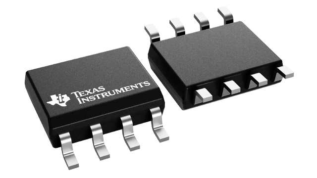
패키징 정보
| 패키지 | 핀 SOIC (D) | 8 |
| 작동 온도 범위(°C) -40 to 125 |
| 패키지 수량 | 캐리어 2,500 | LARGE T&R |
OPA828의 주요 특징
- Low input voltage noise density: 4 nV/√Hz at 1 kHz
- Input voltage noise: 0.1 Hz to 10 Hz: 60 nVRMS
- Low input bias current:
- 0.1 pA (DGN)
- 1 pA (D)
- Input offset voltage:
- 25 µV (DGN)
- 50 µV (D)
- Input offset drift:
- 0.2 µV/°C (DGN)
- 0.45 µV/°C (D)
- MUX-friendly inputs
- Gain bandwidth: 45 MHz
- Slew rate: 150 V/µs
- 14-bit settling time: 120 ns
- Overload power limiter
- Wide supply voltage range: ±4 V to ±18 V
- Packages:
- D Package: 8-pin SOIC
- DGN Package: 8-pin HVSSOP
OPA828에 대한 설명
The OPA828 and OPA2828 ( OPAx828) JFET input operational amplifiers are the next generation OPA627 and OPA827, combining high speed with high dc precision and ac performance. These op amps supply low offset voltage, low drift over temperature, low bias current, and low noise with only 60-nVRMS 0.1-Hz to 10-Hz noise. The OPAx828 operate over a wide supply-voltage range of ±4 V to ±18 V and a supply current of 5.5 mA/channel, typical.
AC characteristics, including a 45-MHz gain bandwidth product (GBW), a slew rate of 150 V/µs, and precision dc characteristics, make the OPAx828 family an excellent choice for a variety of systems. These include high-speed and high-resolution data-acquisition systems, such as 16-bit to 18-bit mixed signal systems, transimpedance (I/V-conversion) amplifiers, filters, precision ±10-V front ends, and high-impedance sensor-interface applications.
The OPAx828 are available in an 8-pin SOIC package and a thermally enhanced, 8-pin HVSSOP PowerPAD™ integrated circuit package.
