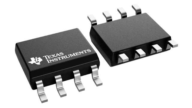
封裝資訊
| 封裝 | 針腳 SOIC (D) | 8 |
| 操作溫度範圍 (°C) |
| 包裝數量 | 運送業者 75 | TUBE |
TLC2201 的特色
- B Grade Is 100% Tested for Noise
- 30 nV/
 Hz Max at f = 10 Hz
 - 12 nV/
 Hz Max at f = 1 kHz
- 30 nV/
- Low Input Offset Voltage . . . 500 µV Max
- Excellent Offset Voltage Stability With Temperature . . . 0.5 µV/°C Typ
- Rail-to-Rail Output Swing
- Low Input Bias Current
- 1 pA Typ at TA = 25°C
- Common-Mode Input Voltage Range Includes the Negative Rail
- Fully Specified For Both Single-Supply and Split-Supply Operation
Advanced LinCMOS is a trademark of Texas Instruments Incorporated.
All other trademarks are the property of their respective owners.
TLC2201 的說明
The TLC220x, TLC220xA, TLC220xB, and TLC220xY are precision, low-noise operational amplifiers using Texas Instruments Advanced LinCMOS™ process. These devices combine the noise performance of the lowest-noise JFET amplifiers with the dc precision available previously only in bipolar amplifiers. The Advanced LinCMOS™ process uses silicon-gate technology to obtain input offset voltage stability with temperature and time that far exceeds that obtainable using metal-gate technology. In addition, this technology makes possible input impedance levels that meet or exceed levels offered by top-gate JFET and expensive dielectric-isolated devices.
The combination of excellent DC and noise performance with a common-mode input voltage range that includes the negative rail makes these devices an ideal choice for high-impedance, low-level signal-conditioning applications in either single-supply or split-supply configurations.
The device inputs and outputs are designed to withstand –100-mA surge currents without sustaining latch-up. In addition, internal ESD-protection circuits prevent functional failures at voltages up to 2000 V as tested under MIL-PRF-38535, Method 3015.2; however, care should be exercised in handling these devices as exposure to ESD may result in degradation of the parametric performance.
The C-suffix devices are characterized for operation from 0°C to 70°C. The I-suffix devices are characterized for operation from –40°C to 85°C. The M-suffix devices are characterized for operation over the full military temperature range of –55°C to 125°C.
