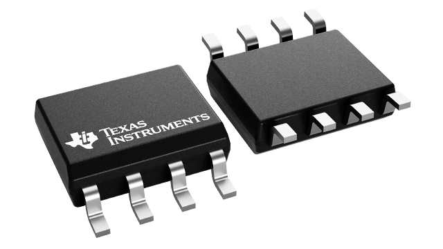
Gehäuseinformationen
| Gehäuse | Pins SOIC (D) | 8 |
| Betriebstemperaturbereich (°C) -40 to 85 |
| Gehäusemenge | Träger 2.500 | LARGE T&R |
Merkmale von SN65LVDS101
- Designed for Signaling Rates ≥ 2 Gbps
- Total Jitter < 65 ps
- Low-Power Alternative for the MC100EP16
- Low 100-ps (Maximum) Part-to-Part Skew
- 25 mV of Receiver Input Threshold Hysteresis
Over 0-V to 4-V Input Voltage Range - Inputs Electrically Compatible With LVPECL,
CML, and LVDS Signal Levels - 3.3-V Supply Operation
- LVDT Integrates 110-Ω Terminating Resistor
- Offered in SOIC and MSOP
Beschreibung von SN65LVDS101
The SN65LVDS100, SN65LVDT100, SN65LVDS101, and SN65LVDT101 are high-speed differential receivers and drivers connected as repeaters. The receiver accepts low-voltage differential signaling (LVDS), positive-emitter-coupled logic (PECL), or current-mode logic (CML) input signals at rates up to 2 Gbps and repeats it as either an LVDS or PECL output signal. The signal path through the device is differential for low radiated emissions and minimal added jitter.
The outputs of the SN65LVDS100 and SN65LVDT100 are LVDS levels as defined by TIA/EIA-644-A. The outputs of the SN65LVDS101 and SN65LVDT101 are compatible with 3.3-V PECL levels. Both drive differential transmission lines with nominally 100-Ω characteristic impedance.
The SN65LVDT100 and SN65LVDT101 include a 110-Ω differential line termination resistor for less board space, fewer components, and the shortest stub length possible. They do not include the VBB voltage reference found in the SN65LVDS100 and SN65LVDS101. VBB provides a voltage reference of typically 1.35 V below VCC for use in receiving single-ended input signals and is particularly useful with single-ended 3.3-V PECL inputs. When VBB is not used, it should be unconnected or open.
All devices are characterized for operation from –40°C to 85°C.
