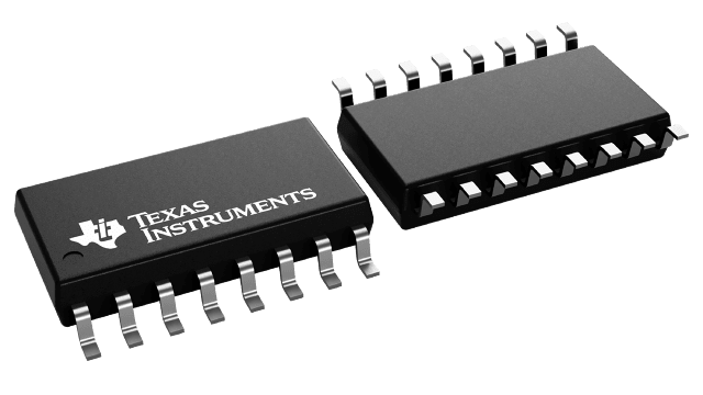
Gehäuseinformationen
| Gehäuse | Pins SOP (NS) | 16 |
| Betriebstemperaturbereich (°C) -20 to 85 |
| Gehäusemenge | Träger 2.000 | LARGE T&R |
Merkmale von SN751177
- Meet or exceed the requirements of ANSI standards TIA/EIA-422-B and TIA/EIA-485-A and ITU recommendations V.10 and V.11
- Designed for multipoint bus transmission on long bus lines in noise environments
- Driver positive- and negative-current limiting
- Thermal shutdown protection
- Driver 3-state outputs
- Receiver common-mode input voltage range of −12V to 12V
- Receiver input sensitivity: ±200mV
- Receiver hysteresis: 50mV typical
- Receiver input impedance: 12 kΩ minimum
- Receiver 3-state outputs (SN751177 only)
- Operate from single 5V supply
Beschreibung von SN751177
The SN751177 and SN751178 dual differential drivers and receivers are monolithic integrated circuits that are designed for balanced multipoint bus transmission at rates up to 10 Mbits. The devices are designed to improve the performance of full-duplex data communications over long bus lines and meet ANSI Standards TIA/EIA-422-B and TIA/EIA-485-A and ITU Recommendations V.10 and V.11.
The SN751177 and SN751178 driver outputs provide limiting for both positive and negative currents and thermal-shutdown protection from line-fault conditions on the transmission bus line.
The receiver features high input impedance of at least 12kΩ, an input sensitivity of ±200mV over a common-mode input voltage range of −12V to 12V, and typical input hysteresis of 50mV. Fail-safe design makes sure the receiver inputs are open, the receiver outputs are always high.
The SN751177 and SN751178 are characterized for operation from −20°C to 85°C.
