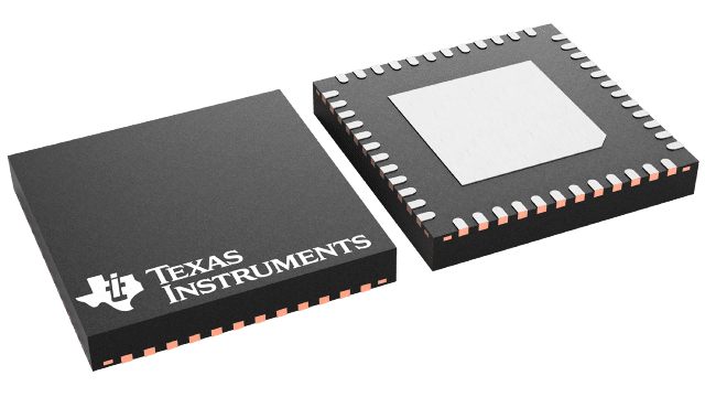
Gehäuseinformationen
| Gehäuse | Pins VQFN (RGZ) | 48 |
| Betriebstemperaturbereich (°C) 0 to 85 |
| Gehäusemenge | Träger 250 | SMALL T&R |
Merkmale von SN75DP159
- AC-coupled TMDS or DisplayPort Dual-Mode Physical Layer Input to HDMI2.0b TMDS Physical Layer Output Supporting up to 6 Gbps Data Rate, Compatible with HDMI2.0b Electrical Parameters
- Supporting DisplayPort Dual-Mode Standard Version 1.1
- Adaptive Receiver Equalizer and Programmable Fixed Equalizer up to 16.5 dB
- High Speed Lane Control, Pre-emphasis and Transmit Swing, and Slew Rate Control
- I2C or Pin Strap Programmable
- Supports Type-2 I2C-over-AUX to DDC Bridge
- Integrated TMDS Level Translator and CDR
- Active I2C[4] Buffer
- Input Swap on Main Lanes
- Low Power Consumption
- Low Power
Consumption
- –435 mW Active at 6-Gbps and –10 mW at Shutdown State
- Both Extended Commercial and Industrial Temperature Device Options
- 40-pin, 0.4 mm Pitch, 5 mm x 5 mm, WQFN Package, Pin Compatible to the TPD158 Redriver
- 40-pin, 0.5 mm Pitch, 7 mm x 7 mm, VQFN Package
Beschreibung von SN75DP159
The SNx5DP159 device is a dual mode[1] DisplayPort to transition-minimized differential signal (TMDS) retimer supporting digital video interface (DVI) 1.0 and high-definition multimedia interface (HDMI) 1.4b and 2.0b output signals. The SNx5DP159 device supports the dual mode standard version 1.1 type 1 and type 2 through the DDC link or AUX channel. The SNx5DP159 device supports data rate up to 6-Gbps per data lane to support Ultra HD (4K × 2K / 60-Hz) 8-bits per color high-resolution video and HDTV with 16-bit color depth at 1080p (1920 × 1080 / 60-Hz). The SNx5DP159 device can automatically configure itself as a re-driver at data rates <1 Gbps, or as a retimer at more than this data rate. This feature can be turned off through I2C[4] programming.
For signal integrity, the SNx5DP159 device implements several features. The SNx5DP159 receiver supports both adaptive and fixed equalization to clean up inter-symbol interference (ISI) jitter or loss from the bandwidth-limited board traces or cables. When working as a retimer, the embedded clock data recovery (CDR) cleans up the input high frequency and random jitter from video source. The transmitter provides several features for passing compliance and reducing system-level design issues like de-emphasis, which compensates for the attenuation when driving long cables or high-loss board traces. The SNx5DP159 device also includes TMDS output amplitude adjust using an external resistor on the Vsadj pin, source termination selection, and output slew rate control. Device operation and configuration can be programmed by pin strapping or I2C[4].
The SNx5DP159 device implements several methods for power management and active power reduction.
The SNx5DP159 receiver uses several methods to determine whether the application supports HDMI1.4b[2] or HDMI2.0[3] data rates. The SNx5DP159 receiver comes in two packages: a 40-pin RSB supporting space-constrained applications and a 48-pin RGZ version supporting the full feature set for DisplayPort dual-mode standard version 1.1 in applications such as dongles.
The SN65DP159 device is characterized for an industrial operational temperature range from –40°C to 85°C.
The SN75DP159 device is characterized for an extended commercial operational temperature range from 0°C to 85°C.
