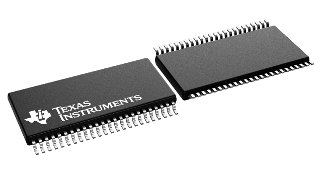
Gehäuseinformationen
| Gehäuse | Pins TSSOP (DGG) | 48 |
| Betriebstemperaturbereich (°C) -40 to 85 |
| Gehäusemenge | Träger 1.000 | LARGE T&R |
Merkmale von DS90CR216A
- 20 to 66 MHz Shift Clock Support
- 50% Duty Cycle on Receiver Output Clock
- Best–in–Class Set and Hold Times on Rx Outputs
- Rx Power Consumption < 270 mW (Typ) at 66
MHz Worst Case - Rx Power-Down Mode < 200 µW (Max)
- ESD Rating > 7 kV (HBM), > 700 V (EIAJ)
- PLL Requires No External Components
- Compatible with TIA/EIA-644 LVDS Standard
- Low Profile 56-Pin or 48-Pin DGG (TSSOP)
Package - Operating Temperature: −40°C to 85°C
- Automotive Q Grade Available – AEC-Q100 Grade
3 Qualified
Beschreibung von DS90CR216A
The DS90CR286A receiver converts the four LVDS data streams back into parallel 28 bits of LVCMOS data. Also available is the DS90CR216A receiver that converts the three LVDS data streams back into parallel 21 bits of LVCMOS data. The outputs of both receivers strobe on the rising edge.
The receiver LVDS clock operates at rates from 20 to 66 MHz. The device phase-locks to the input clock, samples the serial bit streams at the LVDS data lines, and converts them into parallel output data. At an incoming clock rate of 66 MHz, each LVDS input line is running at a bit rate of 462 Mbps, resulting in a maximum throughput of 1.848 Gbps for the DS90CR286A and 1.386 Gbps for the DS90CR216A.
The DS90CR286A and DS90CR216A devices are enhanced over prior generation receivers and provide a wider data valid time on the receiver output. The use of these serial link devices is ideal for solving EMI and cable size problems associated with transmitting data over wide, high speed parallel LVCMOS interfaces. Both devices are offered in TSSOP packages.
