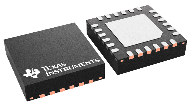
封裝資訊
| 封裝 | 針腳 VQFN (RGE) | 24 |
| 操作溫度範圍 (°C) 0 to 70 |
| 包裝數量 | 運送業者 250 | SMALL T&R |
TLK1002A 的特色
- Fully Integrated Signal Conditioning
Transceiver - 1.0-1.3 Gbps Operation
- Low Power CMOS Design (<300 mW)
- High Differential Output Voltage Swing (1600 mVp-p typical)
- 400 mVp-p Differential Input Sensitivity
- High Input Jitter Tolerance 0.606 UI
- Single 1.8 V Power Supply
- 2.5 V Tolerant Control Inputs
- Differential VML Transmit Outputs With No External Components Necessary
- No External Filter Components Required for PLLs
- Supports Loop-Back Modes
- Temperature Rating 0°C to 70°C
- Small Footprint 4 mm × 4 mm 24-Lead QFN Package
- APPLICATIONS
- Resynchronization in Both Directions for 1.25 Gbps Links
- Repeater for 1.0625 Gbps Applications
TLK1002A 的說明
TLK1002A is a single-chip dual signal conditioning transceiver.
This chip supports data rates from 1.0 Gbps up to 1.3 Gbps. An on-chip clock generation phase-locked loop (PLL) generates the required half-rate clock from an externally applied reference clock. This reference clock equals approximately one tenth of the data rate. It may be off frequency from both received data streams by up to ±200 ppm.
Both data paths are implemented identical. The implemented input buffers provide an input sensitivity of 400 mVp-p differential.
The data paths tolerate up to 0.606 UI total input jitter. Signal retiming is performed by means of phase-locked loop (PLL) circuits. The retimed output signals are fed to VML output buffers, which provide output amplitudes of typical 1600mVp-p differential across the external 2x50  load.
load.
TLK1002A only requires a single 1.8 V supply voltage. Robust design avoids the necessity of special off-chip supply filtering.
Advanced low power CMOS design leads to low power consumption.
