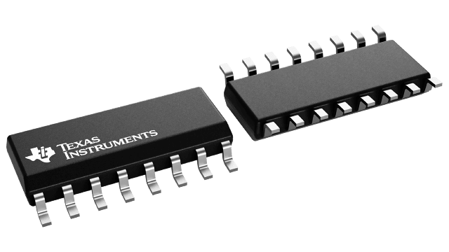
封裝資訊
| 封裝 | 針腳 SOIC (D) | 16 |
| 操作溫度範圍 (°C) 0 to 70 |
| 包裝數量 | 運送業者 40 | TUBE |
UCC3580-2 的特色
- Provides Auxiliary Switch Activation Complementary to Main Power Switch Drive
- Programmable deadtime (Turn-on Delay) Between Activation of Each Switch
- Voltage Mode Control with Feedforward Operation
- Programmable Limits for Both Transformer Volt- Second Product and PWM Duty Cycle
- High Current Gate Driver for Both Main and Auxiliary Outputs
- Multiple Protection Features with Latched Shutdown and Soft Restart
- Low Supply Current (100 µA Startup, 1.5mA Operation)
UCC3580-2 的說明
The UCC3580 family of PWM controllers is designed to implement a variety of active clamp/reset and synchronous rectifier switching converter topologies. While containing all the necessary functions for fixed frequency, high performance pulse width modulation, the additional feature of this design is the inclusion of an auxiliary switch driver which complements the main power switch, and with a programmable deadtime or delay between each transition. The active clamp/reset technique allows operation of single ended converters beyond 50% duty cycle while reducing voltage stresses on the switches, and allows a greater flux swing for the power transformer. This approach also allows a reduction in switching losses by recovering energy stored in parasitic elements such as leakage inductance and switch capacitance.
The oscillator is programmed with two resistors and a capacitor to set switching frequency and maximum duty cycle. A separate synchronized ramp provides a voltage feedforward pulse width modulation and a programmed maximum volt-second limit. The generated clock from the oscillator contains both frequency and maximum duty cycle information.
The main gate drive output (OUT1) is controlled by the pulse width modulator. The second output (OUT2) is intended to activate an auxiliary switch during the off time of the main switch, except that between each transition there is deadtime where both switches are off, programmed by a single external resistor. This design offers two options for OUT2, normal and inverted. In the -1 and -2 versions, OUT2 is normal and can be used to drive PMOS FETs. In the -3 and -4 versions, OUT2 is inverted and can be used to drive NMOS FETs. In all versions, both the main and auxiliary switches are held off prior to startup and when the PWM command goes to zero duty cycle. During fault conditions, OUT1 is held off while OUT2 operates at maximum duty cycle with a guaranteed off time equal to the sum of the two deadtimes.
Undervoltage lockout monitors supply voltage (VDD), the precision reference (REF), input line voltage (LINE), and the shutdown comparator (SHTDWN). If after any of these four have sensed a fault condition, recovery to full operation is initiated with a soft start. VDD thresholds, on and off, are 15V and 8.5V for the -2 and -4 versions, 9V and 8.5V for the -1 and -3 versions.
The UCC1580-x is specified for operation over the military temperature range of –55°C to 125°C. The UCC2580-x is specified from –40°C to 85°C. The UCC3580-x is specified from 0°C to 70°C. Package options include 16-pin surface mount and dual in-line.
