-
Comparing Isolated Amplifiers and Isolated Modulators SBAA359B February 2019 – June 2024 AMC1035 , AMC1035-Q1 , AMC1100 , AMC1106E05 , AMC1106M05 , AMC1200 , AMC1200-Q1 , AMC1203 , AMC1204 , AMC1204-Q1 , AMC1210 , AMC1211-Q1 , AMC1300 , AMC1300B-Q1 , AMC1301-Q1 , AMC1302 , AMC1302-Q1 , AMC1303E0510 , AMC1303E0520 , AMC1303E2510 , AMC1303E2520 , AMC1303M0510 , AMC1303M0520 , AMC1303M2510 , AMC1303M2520 , AMC1304L05 , AMC1304L05-Q1 , AMC1304L25 , AMC1304L25-Q1 , AMC1304M05 , AMC1304M05-Q1 , AMC1304M25 , AMC1304M25-Q1 , AMC1305L25 , AMC1305L25-Q1 , AMC1305M05 , AMC1305M05-Q1 , AMC1305M25 , AMC1305M25-Q1 , AMC1306E05 , AMC1306E25 , AMC1306M05 , AMC1306M25 , AMC1311 , AMC1311-Q1 , AMC1336 , AMC1336-Q1 , AMC1411 , AMC3301 , AMC3301-Q1 , AMC3302 , AMC3302-Q1 , AMC3306M05 , AMC3306M25 , AMC3330 , AMC3330-Q1 , AMC3336 , AMC3336-Q1 , ISO121 , ISO122 , ISO124 , ISO224
-
Comparing Isolated Amplifiers and Isolated Modulators
- 1
- Abstract
- Trademarks
- 1Introduction to Isolated Amplifiers
- 2Introduction to Isolated Modulators
- 3Performance Comparison Between Isolated Amplifiers and Isolated Modulators
- 4Isolated Modulators in Traction Inverters
- 5Isolated Amplifier and Modulator Recommendations
- 6Conclusion
- 7Revision History
- IMPORTANT NOTICE
Comparing Isolated Amplifiers and Isolated Modulators
Abstract
Industrial applications such as motor drives, photo voltaic inverters, and uninterruptible power supplies (UPS) and automotive applications such as onboard chargers (OBCs), traction inverters, and DC/DC converters operate at high voltage and current levels to optimize overall efficiency and power throughput. These systems are subjected to hostile environments such as electrical noise, vibration, mechanical shock, extreme temperatures, ingress of contaminants, and so forth. Such systems demand robust, reliable, galvanic isolation to isolate high voltages from low-voltage circuits. The feedback signals measured on these high voltages are galvanically isolated from the low-voltage controllers by isolated amplifiers or isolated modulators.
This document compares isolated amplifiers and isolated-modulator-based designs and explains some unique advantages of isolated-modulator-based designs.
Trademarks
All trademarks are the property of their respective owners.
1 Introduction to Isolated Amplifiers
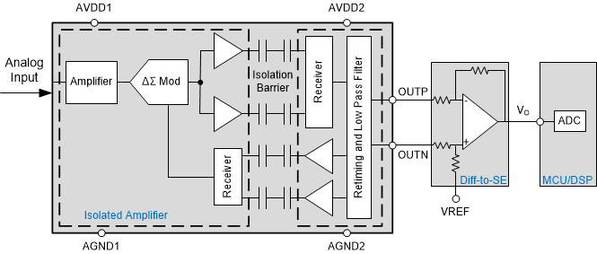
Figure 1-1 shows the implementation of an isolated-amplifier-based measurement design.
 Figure 1-1 Isolated Amplifier Implementation
The input stage of an isolated amplifier consists of an input amplifier that drives a delta-sigma (ΔΣ) modulator. The gain of the input amplifier is fixed and set by internal precision resistors. The ΔΣ modulator uses the internal reference voltage and clock generator to convert the analog input signal to a digital bit stream. The drivers transfer the output of the modulator across an isolation barrier that separates the high and low voltage domains. The received bitstream and clock are synchronized and processed by an analog low-pass filter on the low voltage side and presented as an analog output signal.
The differential output of the isolated amplifier is often converted to a single-ended analog output with an op-amp-based circuit. This op-amp-based circuit can also implement a low-pass filter to further reduce the signal bandwidth to a bandwidth of interest and thereby improve the system noise performance.
The analog-to-digital converter (ADC), either external or internal to the microcontroller (MCU) or digital signal processor (DSP), receives this feedback analog output and converts this output back to the digital domain.