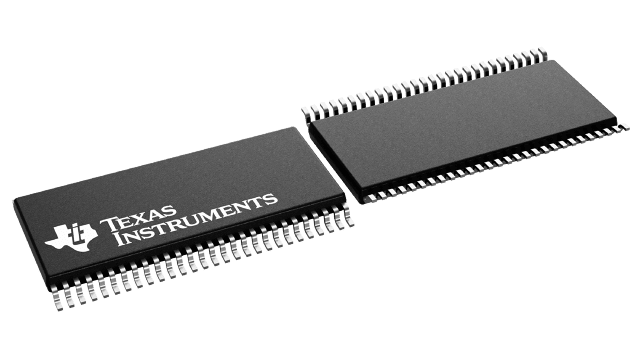
Gehäuseinformationen
| Gehäuse | Pins TSSOP (DGG) | 56 |
| Betriebstemperaturbereich (°C) -40 to 85 |
| Gehäusemenge | Träger 34 | TUBE |
Merkmale von DS90CF384
- 20 to 65 MHz shift clock support
- Programmable transmitter (DS90C383) strobe select
(Rising or Falling edge strobe) - Single 3.3V supply
- Chipset (Tx + Rx) power consumption < 250 mW (typ)
- Power-down mode (< 0.5 mW total)
- Single pixel per clock XGA (1024x768) ready
- Supports VGA, SVGA, XGA and higher addressability.
- Up to 227 Megabytes/sec bandwidth
- Up to 1.8 Gbps throughput
- Narrow bus reduces cable size and cost
- 290 mV swing LVDS devices for low EMI
- PLL requires no external components
- Low profile 56-lead TSSOP package.
- DS90CF384 also available in 64 ball, 0.8mm fine pitch
ball grid array(FBGA) package - Falling edge data strobe Receiver
- Compatible with TIA/EIA-644 LVDS standard
- ESD rating >7 kV
- Operating Temperature: –40°C to +85°C
Beschreibung von DS90CF384
The DS90C383 transmitter converts 28 bits of CMOS/TTL data into four LVDS (Low Voltage Differential Signaling) data streams. A phase-locked transmit clock is transmitted in parallel with the data streams over a fifth LVDS link. Every cycle of the transmit clock 28 bits of input data are sampled and transmitted. The DS90CF384 receiver converts the LVDS data streams back into 28 bits of CMOS/TTL data. At a transmit clock frequency of 65 MHz, 24 bits of RGB data and 3 bits of LCD timing and control data (FPLINE, FPFRAME, DRDY) are transmitted at a rate of 455 Mbps per LVDS data channel. Using a 65 MHz clock, the data throughputs is 227 Mbytes/sec. The transmitter is offered with programmable edge data strobes for convenient interface with a variety of graphics controllers. The transmitter can be programmed for Rising edge strobe or Falling edge strobe through a dedicated pin. A Rising edge transmitter will inter-operate with a Falling edge receiver (DS90CF384) without any translation logic. The DS90CF384 is also offered in 64 ball, 0.8mm fine pitch ball grid array(FBGA) package which provides a 44 % reduction in PCB footprint (available Q3, 1999).
This chipset is an ideal means to solve EMI and cable size problems associated with wide, high speed TTL interfaces.
