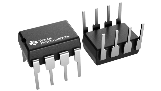
Gehäuseinformationen
| Gehäuse | Pins PDIP (P) | 8 |
| Betriebstemperaturbereich (°C) 0 to 70 |
| Gehäusemenge | Träger 40 | TUBE |
Merkmale von LF398-N
- Operates from ±5-V to ±18-V Supplies
- Less than 10-µs Acquisition Time
- Logic Input Compatible With TTL, PMOS, CMOS
- 0.5-mV Typical Hold Step at Ch = 0.01 µF
- Low Input Offset
- 0.002% Gain Accuracy
- Low Output Noise in Hold Mode
- Input Characteristics Do Not Change During Hold Mode
- High Supply Rejection Ratio in Sample or Hold
- Wide Bandwidth
- Space Qualified, JM38510
Beschreibung von LF398-N
The LFx98x devices are monolithic sample-and-hold circuits that use BI-FET technology to obtain ultrahigh DC accuracy with fast acquisition of signal and low droop rate. Operating as a unity-gain follower, DC gain accuracy is 0.002% typical and acquisition time is as low as 6 µs to 0.01%. A bipolar input stage is used to achieve low offset voltage and wide bandwidth. Input offset adjust is accomplished with a single pin and does not degrade input offset drift. The wide bandwidth allows the LFx98x to be included inside the feedback loop of 1-MHz operational amplifiers without having stability problems. Input impedance of 1010 Ω allows high-source impedances to be used without degrading accuracy.
P-channel junction FETs are combined with bipolar devices in the output amplifier to give droop rates as low as 5 mV/min with a 1-µF hold capacitor. The JFETs have much lower noise than MOS devices used in previous designs and do not exhibit high temperature instabilities. The overall design ensures no feedthrough from input to output in the hold mode, even for input signals equal to the supply voltages.
Logic inputs on the LFx98x are fully differential with low input current, allowing for
direct connection to TTL, PMOS, and CMOS. Differential threshold is
1.4 V. The LFx98x will operate from ±5-V to ±18-V supplies.
An A version is available with tightened electrical specifications.
