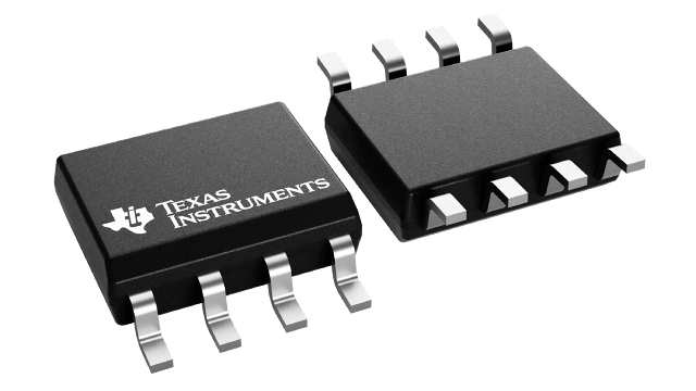
패키징 정보
| 패키지 | 핀 SOIC (D) | 8 |
| 작동 온도 범위(°C) |
| 패키지 수량 | 캐리어 75 | TUBE |
TPS766의 주요 특징
- Input voltage range:
- Legacy chip: 2.7V to 10V (13.5V absolute max)
- New chip: 2.5V to 16V (18V absolute max)
- Output voltage range:
- Legacy chip: 1.5V to 5V (fixed) and 1.25V to 5.5V (adjustable)
- New chip: 1.2V to 12V (fixed) and 0.8V to 14.6V (adjustable)
- Output current: Up to 250mA
- Output accuracy:
- Legacy chip: 3% over load and temperature
- New chip: 1% over load and temperature
- Low quiescent current (IQ):
- Legacy chip: 35µA (typ) with no load
- New chip: 55µA (typ) with no load
- IQ (disabled
state):
- Legacy chip: 10µA (max)
- New chip: 4µA (max)
- Dropout voltage (new chip):
- Up to 225mV (typ) at 250mA (TPS76650)
- High PSRR (new chip): 46dB at 1MHz
- Internal soft-start time (new chip): 750µs (typical)
- Overcurrent limiting and thermal protection
- Stable with a 2.2µF or larger capacitor (new chip)
- Open-drain power-good
- Package: 8-pin, 4.9mm × 6mm SOIC (D)
TPS766에 대한 설명
The TPS766 is a low-dropout (LDO) linear voltage regulator that supports an input voltage range from 2.5V to 16V (new chip) and up to 250mA of load current. For the new chip, the supported output range is from 1.2V to 12V (fixed version) or from 0.8V to 14.6V (adjustable version).
The input voltage range is up to 16V (new chip), which makes the device a good choice for operating from transformer secondary windings and regulated rails (such as 10V or 12V). Additionally, the wide output voltage range allows the device to generate the bias voltage for silicon carbide (SiC) gate drivers and microphones, as well as power microcontrollers (MCUs) and processors.
Wide bandwidth PSRR performance is greater than 70dB at 1kHz and 46dB at 1MHz (new chip), which helps attenuate the switching frequency of an upstream DC/DC converter and minimizes post regulator filtering. The new chip supports internal soft-start circuit mechanism that reduces inrush current during start-up, thus allowing for smaller input capacitance.
The legacy chip supports constant quiescent current across the complete load current range (typically 35µA for the full range of output current, 0mA to 250mA).
The TPS766 LDO also features a sleep mode, where applying a TTL high signal to EN (enable) shuts down the regulator. In disabled mode, the quiescent current for the legacy chip is less than 1µA (typ) and the quiescent current for the new chip is approximately 1.6µA (typ).
Power-good (PG) is an active-high output used to implement a power-on reset or a low-battery indicator.
For the fixed-output version, The TPS766 provides an output range of 1.5V to 5.0V (legacy chip) and 1.2V to 12V (new chip). For the adjustable version, program the output voltage over the range of 1.25V to 5.5V (legacy chip) and 0.8V to 14.6V (new chip). The TPS766 is available in an 8-pin SOIC package.
