SBAA534 March 2022 ADC128S102-SEP , ADC128S102QML-SP , ADS1278-SP , ADS1282-SP , LF411QML-SP , LM101AQML-SP , LM111QML-SP , LM119QML-SP , LM124-SP , LM124AQML-SP , LM136A-2.5QML-SP , LM139-SP , LM139AQML-SP , LM148JAN-SP , LM158QML-SP , LM185-1.2QML-SP , LM185-2.5QML-SP , LM193QML-SP , LM4050QML-SP , LM6172QML-SP , LM7171QML-SP , LMH5401-SP , LMH5485-SEP , LMH5485-SP , LMH6628QML-SP , LMH6702QML-SP , LMH6715QML-SP , LMP2012QML-SP , LMP7704-SP , OPA4277-SP , OPA4H014-SEP , OPA4H199-SEP , THS4304-SP , THS4511-SP , THS4513-SP , TL1431-DIE , TL1431-SP , TLC2201-SP , TLV1704-SEP , TLV4H290-SEP , TLV4H390-SEP
2.1 Detailed Design Procedure – Verification of the Time Domain Response
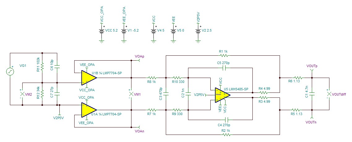
As Figure 2-1 shows, before the verification analysis can start, the design must first complete the attenuation and input buffer stage. The important design goals to remember here are a single-ended ±10-V input signal is translated into a ± 2.5-V differential signal for the ADC input and the input impedance must be > 100 kΩ.
For the input buffer, the LMP7704-SP device was selected. The resistor divider network of the attenuation stage brings the signal level down by a factor of four. The input signal generator VG1 is set to 240-kHz sine wave with ±10-V amplitude.
 Figure 2-1 Addition of Attenuation Stage
and Input Buffer Stage to the FDA Circuit
Figure 2-1 Addition of Attenuation Stage
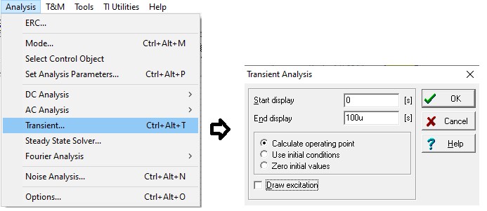
and Input Buffer Stage to the FDA CircuitFigure 2-2 shows the selection of Transient… in the Analysis menu of TINA-TI and setting the simulation window from "0" to "100u" (100 μs).
 Figure 2-2 Running the Transient Analysis
From 0 to 100 μs
Figure 2-2 Running the Transient Analysis
From 0 to 100 μsThe returned waveform in Figure 2-3 shows that the single-ended input signal with an amplitude of 10 V results into a differential output signal with an amplitude of 2.5 V. This amplitude takes advantage of the full input voltage range of the ADC for the best possible resolution.
 Figure 2-3 Simulation of FDA Output
Voltage VOUTdiff Versus Input Signal VG1