SBAA534 March 2022 ADC128S102-SEP , ADC128S102QML-SP , ADS1278-SP , ADS1282-SP , LF411QML-SP , LM101AQML-SP , LM111QML-SP , LM119QML-SP , LM124-SP , LM124AQML-SP , LM136A-2.5QML-SP , LM139-SP , LM139AQML-SP , LM148JAN-SP , LM158QML-SP , LM185-1.2QML-SP , LM185-2.5QML-SP , LM193QML-SP , LM4050QML-SP , LM6172QML-SP , LM7171QML-SP , LMH5401-SP , LMH5485-SEP , LMH5485-SP , LMH6628QML-SP , LMH6702QML-SP , LMH6715QML-SP , LMP2012QML-SP , LMP7704-SP , OPA4277-SP , OPA4H014-SEP , OPA4H199-SEP , THS4304-SP , THS4511-SP , THS4513-SP , TL1431-DIE , TL1431-SP , TLC2201-SP , TLV1704-SEP , TLV4H290-SEP , TLV4H390-SEP
1 Component and Topology Selection - Finding a Good Starting Point Quickly
The following chapters use an example design described by Table 1-1.
| Parameter | Design Goal |
|---|---|
| Channel Count | 8 |
| Bandwidth and Sampling Rate | 40 kHz, > 100 ksps |
| Input Full Scale Range (FSR) | ±10-V FSR |
|
Common-Mode Voltage |
About 0 V common mode |
|
Target Resolution, ENOB |
> 16 bit |
|
Input Impedance (ZIN) Target |
> 100 kΩ |
|
Radiation hardness |
TID: > 50 krad, SEL: > 60 (MeV × cm2/mg) |
The TI Space Products Guide, Space-Grade Data Converters section shows that the ADS1278-SP best fits these requirements.
 Figure 1-1 TI’s Space-Grade Precision
ADCs Listed in TI's Space Product Guide
Figure 1-1 TI’s Space-Grade Precision
ADCs Listed in TI's Space Product GuideThe next step is to identify the right ADC driver. For best noise immunity and linearity a fully differential amplifier (FDA) is preferred.
To identify the right product, the minimum unity gain bandwidth of such FDA must be understood. The ANALOG-ENGINEER’S CALCULATOR provides great assistance here.
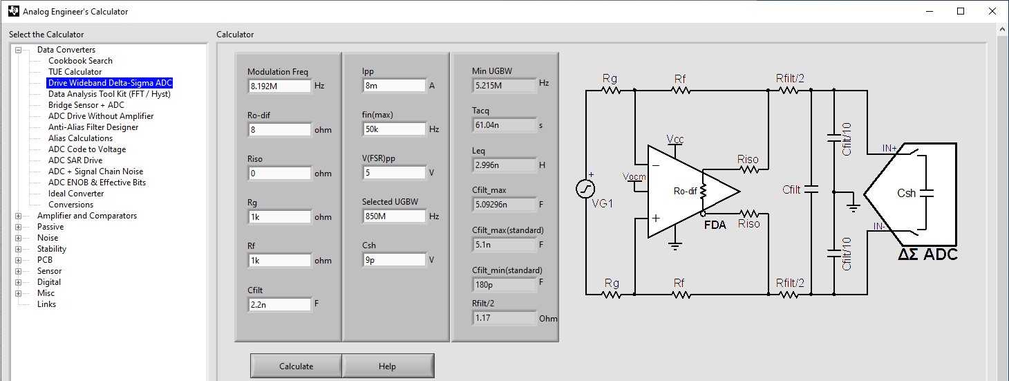 Figure 1-2 ANALOG-ENGINEER’S CALCULATOR –
Drive Wideband Delta-Sigma ADC
Figure 1-2 ANALOG-ENGINEER’S CALCULATOR –
Drive Wideband Delta-Sigma ADCFigure 1-2 illustrates that the Data Converters menu offers the Drive Wideband Delta-Sigma ADC item. The reference schematic in the figure shows all relevant component values. The white fields must be entered by the user, the gray fields are the resulting values. The very first variable to define is the minimum unity gain bandwidth (UGBW). In other words, up to what frequency must the gain of the amplifier be equal or greater than one. Since the ADC will cut off any information above the Nyquist or sample frequency divided by two, it is sufficient if the UGBW of the amplifier is about two-thirds of the sampling frequency. For example, for a sample rate of 1 kHz, look at a minimum UGBW of 636.6 Hz.
The selected ADC in the example of this report is a sigma-delta ADC. It is important to remember that a sigma-delta ADC is a one-bit ADC at the provided modulation frequency. The actual sample rate is only the frequency the full sample words come out of it. The relevant frequency for the AFE design is the modulation frequency which is much higher.
Due to the flexibility and complexity of modern ADCs it is not always straightforward to read the modulation frequency from the data sheet. The ADS1278-SP provides different operating modes that allow for different master clock rates. Figure 1-3 shows the actual modulation frequency is just one-fourth of the master clock. In the example, the ADS1278-SP operates in High-Speed mode: 128 ksps, fCLK is 32.786 MHz. FCLK divided by four results in 8.192 MHz for the actual modulation frequency.
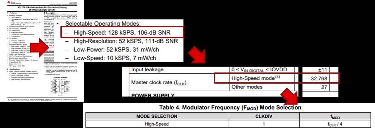 Figure 1-3 Reading the Modulation
Frequency From the ADS1278-SP Data Sheet
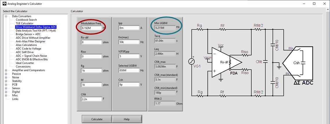 Figure 1-4 Using ANALOG-ENGINEER’S
CALCULATOR to Determine the Minimum Unity Gain Bandwidth of the FDA
Figure 1-4 Using ANALOG-ENGINEER’S
CALCULATOR to Determine the Minimum Unity Gain Bandwidth of the FDAFigure 1-5 illustrates the TI space product guide showing four FDAs. All four provide more than sufficient UGBW. As an example for this report, the lowest one (LMH5485-SP) with 850-MHz UGBW is selected.
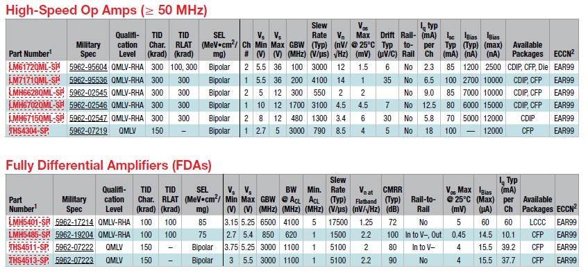 Figure 1-5 Selecting the Best Fitting FDA
from TI’s Space Product Guide
Figure 1-5 Selecting the Best Fitting FDA
from TI’s Space Product GuideWith that selection it is now possible to fill the rest of the white fields in the ANALOG-ENGINEER’S CALCULATOR, see Figure 1-6.
| Parameter | Description |
|---|---|
| Ro-dif | Ro-dif is the
“open-loop output impedance”. The LMH5485-SP Radiation
Hardened Assured (RHA) Negative Rail Input, Rail-to-Rail
Output, Precision, 850 MHz Fully Differential
Amplifier data sheet provides only the closed-loop
output impedance = 0.1 Ω. The Small-Signal Frequency Response vs Gain graph in the Typical Characteristics: 5 V Single Supply section of the LMH5485-SP data sheet provides the gain versus frequency curve. For the modulation frequency of 8.192 MHz, the graph shows about 38 dB, that is, about 80. With the relation of Ro-dif calculates as follows: 90 × 0.1 Ω = 8 Ω. |
| Riso | Riso is typically tuned to a small value. Here "0" (0 Ω) is used. |
| Rg and Rf | Rg and Rf must be the same for unity gain. "1k" (1 kΩ) is typically a good starting point. |
| IPP | The LMH5485-SP data sheet allows for up to 75 mA of output current. An unnecessarily high output current would cause power loss and heating of the FDA which may cause a drift from the optimal working point. A value of "8m" (8 mA) is enough to make calculations in this example. |
| fin | The required bandwidth is 40 kHz. With some margin, "50k" (50 kHz) is a good selection here. |
| UGBW | The UGBW of FDA is "859M" (850 MHz). |
| CSH | Use CSH from the Equivalent Analog Input Circuitry image in the ADS1278-SP Radiation Hardened 8-Ch Simultaneous-Sampling 24-Bit Analog-to-Digital Converter data sheet: "9p" (9 pF). |
| CFILT | Prior defining leaves CFILT as the last entries - press the Calculate button to obtain the updated values for Cfilt_min "180p" (180 pF) and Cfilt_max "5.1n" (5.1 nF). Use "2.2n" (2.2 nF) as the value somewhat in between 5 nF and 180 pF. |
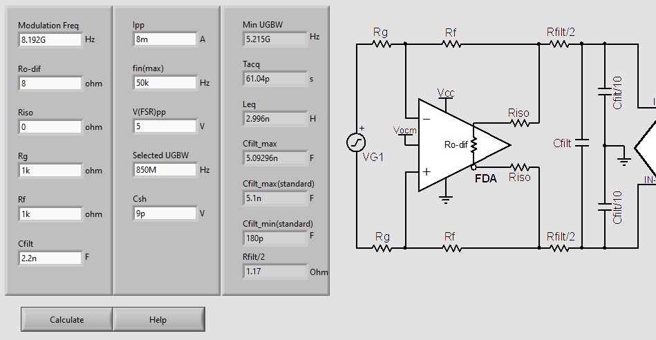 Figure 1-6 User Defined And Calculated
Values For The Reference Schematic With LMH5485-SP and ADS1278-SP to Meet the
Example Design Targets
Figure 1-6 User Defined And Calculated
Values For The Reference Schematic With LMH5485-SP and ADS1278-SP to Meet the
Example Design TargetsIn this chapter the best fitting ADC and ADC-driver was selected with the help of the TI Space Products Guide and the ANALOG-ENGINEER’S CALCULATOR was used to determine its supporting circuitry, including all component values. Further, a basic understanding of the circuit and the role of each of the active and passive components was developed.