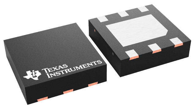
Gehäuseinformationen
| Gehäuse | Pins WSON (NGG) | 6 |
| Betriebstemperaturbereich (°C) -40 to 125 |
| Gehäusemenge | Träger 1.000 | SMALL T&R |
Merkmale von LP38693-ADJ-Q1
- Wide Input Voltage Range: 2.7 V to 10 V
- All WSON Options are Available as AEC-Q100 Grade 1
- Output Voltage Range: 1.25 V to 9 V
- 2% Adjust (ADJ) Pin Voltage Accuracy (25°C)
- Low Dropout Voltage: 250 mV at 500 mA
(Typical, 5-V Out) - Precision (Trimmed) Bandgap Reference
- Ensured Specs for –40°C to 125°C
- 1-µA Off-State Quiescent Current
- Thermal Overload Protection
- Foldback Current Limiting
- Ground (GND) Pin Curent: 55 µA (Typical) at Full Load
- Enable (EN) Pin (LP38693-ADJ)
Beschreibung von LP38693-ADJ-Q1
The LP3869x-ADJ low-dropout CMOS linear regulators provide 2% precision reference voltage, extremely low dropout voltage (250 mV at 500-mA load current, VOUT = 5 V), and excellent AC performance using ultra-low equivalent series resistance (ESR) ceramic output capacitors.
The low thermal resistance of the WSON and SOT-223 packages allow use of the full operating current even in high ambient temperature environments.
The use of a PMOS power transistor means that no DC base drive current is required to bias it, thus allowing the GND-pin current to remain below 100 µA regardless of load current, input voltage, or operating temperature.
For all available packages, see the orderable addendum at the end of the data sheet.