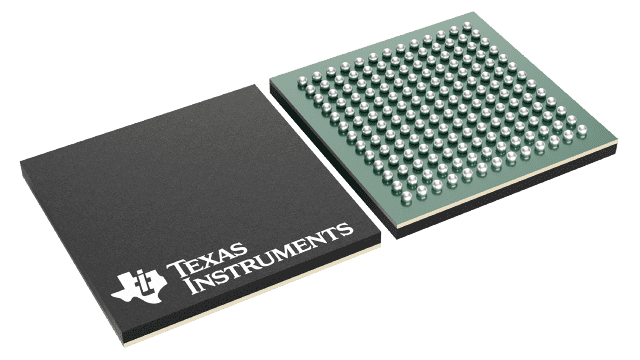
Gehäuseinformationen
| Gehäuse | Pins NFBGA (ZWS) | 169 |
| Betriebstemperaturbereich (°C) -40 to 85 |
| Gehäusemenge | Träger 1.000 | LARGE T&R |
Merkmale von TPS659037
- Seven Step-Down Switched-Mode Power Supply (SMPS)
Regulators:
- One 0.7 to 1.65 V at 6 A (10-mV
Steps)
- Dual-Phase Configuration With Digital Voltage Scaling (DVS) Control
- One 0.7 to 1.65 V at 4 A (10-mV
Steps)
- Dual-Phase Configuration With DVS Control
- One 0.7 to 3.3 V at 3 A (10 or 20-mV
Steps)
- Single-Phase Configuration
- This Regulator can be Combined With the 6 A Resulting in a 9-A Triple-Phase Regulator (DVS Controlled)
- Two 0.7 to 3.3 V at 2 A (10 or 20-mV
Steps)
- Single-Phase Configuration
- One Regulator With DVS Control That can also be Configured as a 3-A Regulator
- Two 0.7 to 3.3 V at 1 A (10 or 20-mV
Steps)
- Single-Phase Configuration
- One Regulator With DVS Control
- Output Current Measurement in All Except 1-A SMPS Regulators
- Differential Remote Sensing (Output and Ground) in Dual-Phase and Triple-Phase Regulators
- Hardware and Software-Controlled Eco-mode™ up to 5 mA with 15-µA Quiescent Current
- Short-Circuit Protection
- Powergood Indication (Voltage and Overcurrent Indication)
- Internal Soft-Start for In-Rush Current Limitation
- Ability to synchronize SMPS to External Clock or Internal Fallback Clock With Phase Synchronization
- One 0.7 to 1.65 V at 6 A (10-mV
Steps)
- Seven
General-Purpose Low Dropout Regulators (LDOs) with 50-mV Steps:
- Two 0.9 to 3.3-V LDOs at 300 mA With Preregulated Supply
- Two 0.9 to 3.3-V LDOs at 200 mA With Preregulated Supply
- One 0.9 to 3.3-V LDOs at 50 mA With Preregulated Supply
- One 100-mA USB LDO
- One 0.9 to 3.3-V, Low-Noise LDO up to 100 mA (Low-Noise Performance up to 50 mA)
- Two Additional LDOs for PMU Internal Use
- Short-Circuit Protection
- Clock Management 16-MHz Crystal Oscillator
and 32-kHz RC Oscillator
- One Buffered 32-kHz Output
- Real-Time Clock (RTC) With Alarm Wake-Up Mechanism
- 12-bit Sigma-Delta General-Purpose Analog-to-Digital-Converter (GPADC) With Three External Input Channels and Six Internal Channels for Self Monitoring
- Thermal Monitoring
- High Temperature Warning
- Thermal Shutdown
- Control
- Configurable Power-Up and Power-Down Sequences (One-Time Programmable [OTP])
- Configurable Sequences Between the SLEEP and ACTIVE States (OTP Programmable)
- One Dedicated Digital Output Signal (REGEN) that can be Included in the Start-Up Sequence
- Three Digital Output Signals MUXed With GPIO that can be Included in the Start-Up Sequence
- Selectable Control Interface
- One Serial Peripheral Interface (SPI) for Resource Configurations and DVS Control
- Two I2C Interfaces. One Dedicated for DVS Control, and a General Purpose I2C Interface for Resource Configuration and DVS Control
- Undervoltage Lockout
- System Voltage Range from 3.135 to 5.25 V
- Package
Options
- 12-mm × 12-mm 169-pin nFBGA with 0,8-mm Pin Pitch
Beschreibung von TPS659037
The TPS659037 device is an integrated power-management IC (PMIC). The device provides seven configurable step-down converters with up to 6 A of output current for memory, processor core, input-output (I/O), or preregulation of LDOs. One of these configurable step-down converters can be combined with another 3-A regulator to allow up to 9 A of output current. All of the step-down converters can synchronize to an external clock source between 1.7 MHz and 2.7 MHz, or an internal fallback clock at 2.2 MHz.
The TPS659037 device contains seven LDO regulators for external use. These LDO regulators can be supplied from either a system supply or a preregulated supply. The power-up and power-down controller is configurable and supports any power-up and power-down sequences (OTP based). The TPS659037 device includes a 32-kHz RC oscillator to sequence all resources during power up and power down. In cases where a fast start up is needed, a 16-MHz crystal oscillator is also included to quickly generate a stable 32-kHz for the system. All LDOs and SMPS converters can be controlled by the SPI or I2C interface, or by power request signals. In addition, voltage scaling registers allow transitioning the SMPS to different voltages by SPI, I2C, or roof and floor control.
One dedicated pin in each package can be configured as part of the power-up sequence to control external resources. General-purpose input-output (GPIO) functionality is available and two GPIOs can be configured as part of the power-up sequence to control external resources. Power request signals enable power mode control for power optimization. The device includes a general-purpose sigma-delta analog-to-digital converter (GPADC) with three external input channels.
The TPS659037 device is available in a 13-pin × 13-pin nFBGA package with a 0,8-mm pitch.