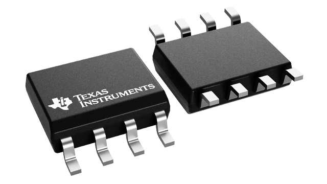
패키징 정보
| 패키지 | 핀 SOIC (D) | 8 |
| 작동 온도 범위(°C) -40 to 125 |
| 패키지 수량 | 캐리어 75 | TUBE |
TPS28226의 주요 특징
- Drives Two N-Channel MOSFETs with 14-ns Adaptive Dead Time
- Wide Gate Drive Voltage: 4.5 V Up to 8.8 V With Best Efficiency at 7 V to 8 V
- Wide Power System Train Input Voltage: 3 V Up to 27 V
- Wide Input PWM Signals: 2.0 V up to 13.2-V Amplitude
- Capable to Drive MOSFETs with ≥40-A Current per Phase
- High Frequency Operation: 14-ns Propagation Delay and 10-ns Rise/Fall Time Allow FSW – 2 MHz
- Capable to Propagate <30-ns Input PWM Pulses
- Low-Side Driver Sink On-Resistance (0.4 Ω) Prevents dV/dT Related Shoot-Through Current
- 3-State PWM Input for Power Stage Shutdown
- Space Saving Enable (Input) and Power Good (Output) Signals on Same Pin
- Thermal Shutdown
- UVLO Protection
- Internal Bootstrap Diode
- Economical SOIC-8 and Thermally Enhanced 3-mm x 3-mm DFN-8 Packages
- High Performance Replacement for Popular 3-State Input Drivers
TPS28226에 대한 설명
The is a high-speed driver for N-channel complimentary driven power MOSFETs with adaptive dead-time control. This driver is optimized for use in variety of high-current one and multi-phase DC-to-DC converters. The is a solution that provides high efficiency, small size and low EMI emissions.
The efficiency is achieved by up to 8.8-V gate drive voltage, 14-ns adaptive dead-time control, 14-ns propagation delays and high-current 2-A source and 4-A sink drive capability. The 0.4-Ω impedance for the lower gate driver holds the gate of power MOSFET below its threshold and ensures no shoot-through current at high dV/dt phase node transitions. The bootstrap capacitor charged by an internal diode allows use of N-channel MOSFETs in a half-bridge configuration.
