SLVA959B November 2018 – October 2021 DRV10866 , DRV10963 , DRV10964 , DRV10970 , DRV10974 , DRV10975 , DRV10983 , DRV10983-Q1 , DRV10987 , DRV11873 , DRV3205-Q1 , DRV3220-Q1 , DRV3245E-Q1 , DRV3245Q-Q1 , DRV8301 , DRV8302 , DRV8303 , DRV8304 , DRV8305 , DRV8305-Q1 , DRV8306 , DRV8307 , DRV8308 , DRV8312 , DRV8313 , DRV8320 , DRV8320R , DRV8323 , DRV8323R , DRV8343-Q1 , DRV8350 , DRV8350R , DRV8353 , DRV8353R , DRV8412 , DRV8701 , DRV8702-Q1 , DRV8702D-Q1 , DRV8703-Q1 , DRV8703D-Q1 , DRV8704 , DRV8711 , DRV8800 , DRV8801 , DRV8801-Q1 , DRV8801A-Q1 , DRV8802 , DRV8802-Q1 , DRV8803 , DRV8804 , DRV8805 , DRV8806 , DRV8811 , DRV8812 , DRV8813 , DRV8814 , DRV8816 , DRV8818 , DRV8821 , DRV8823 , DRV8823-Q1 , DRV8824 , DRV8824-Q1 , DRV8825 , DRV8828 , DRV8829 , DRV8830 , DRV8832 , DRV8832-Q1 , DRV8833 , DRV8833C , DRV8834 , DRV8835 , DRV8836 , DRV8837 , DRV8837C , DRV8838 , DRV8839 , DRV8840 , DRV8841 , DRV8842 , DRV8843 , DRV8844 , DRV8846 , DRV8847 , DRV8848 , DRV8850 , DRV8860 , DRV8870 , DRV8871 , DRV8871-Q1 , DRV8872 , DRV8872-Q1 , DRV8873-Q1 , DRV8880 , DRV8881 , DRV8884 , DRV8885 , DRV8886 , DRV8886AT , DRV8889-Q1
1.1 Frequently Used Terms/Connections
The terms used in this section are defined as follows:
- Single PointIn single-point distribution, all references points originate from the source which makes sure each resource has its own uninterrupted ground path (see Figure 1-1). This connection is recommended for power distribution traces.
- Star GroundIn star-ground distribution, all reference points are located centrally; however, the source may not be centralized. This method balances the common impedance across all resources (Figure 1-1). This connection is recommended for signal traces.
 Figure 1-1 Star-Ground and Single-Point Power Distribution
- PartitioningIn a partitioning ground scheme, the layout of the printed circuit board (PCB) is such that the digital, analog, and high power signals have their own separate areas (see Figure 1-2). This separation is not a physical partition of digital and analog ground.
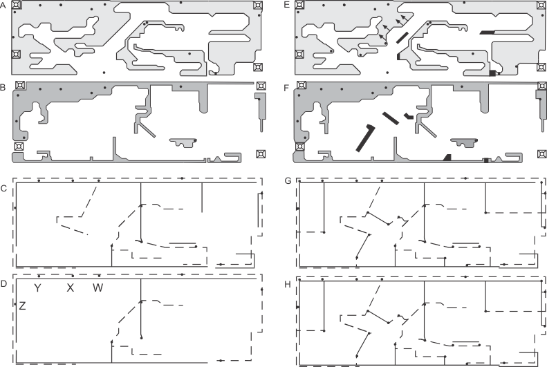
- GridGridding makes the ground paths continuous throughout the board to make sure each signal has a return path to the source (see Figure 1-3). This practice involves making small changes to the component placement, ground fill , via placements, and trace paths to minimize the return path to ground. Gridding effectively creates a more interconnected ground plane, which can decrease noise and lower the impedance between the supply and load.
 Figure 1-2 Digital - Analog Separation and Ground Partition
An example of using ground gridding to achieve an effective ground plane is shown in Figure 1-3. The changes made to implement gridding in the layout were minor, indicating how a small effort can have a large impact.

In the example in Figure 1-3, layout A and layout B are the top and bottom layers, leaving only the ground fill, ground traces and the vias between the front and back. Layout C in Figure 1-3 is a simple stick diagram of the ground routing for the board. Each stick, or leg, represents the path of the ground conductor. Most traces are connected at only one end. With most of the single-ended traces removed, the layout D in Figure 1-3 shows how ground is routed over the entire board; only one path occurs between any two points anywhere on the routing.
Layout E, Layout F, Layout G, and Layout H in Figure 1-3 shows the design modified to achieve a gridded ground. Some traces (show in solid black) were added and geometries were moved (indicated by the arrows) in layout E and layout F in Figure 1-3. Layout G in Figure 1-3 shows the modified stick diagram of ground. Full traces connected at both ends form a more complete conductor. Compare layout H and layout D in Figure 1-3. The gridding ground has created an extensive network of interconnections that creates the desired grid. The result is nearly as effective as an actual ground plane.