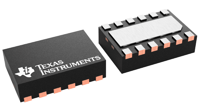
Gehäuseinformationen
| Gehäuse | Pins WSON (DSS) | 12 |
| Betriebstemperaturbereich (°C) -40 to 125 |
| Gehäusemenge | Träger 3.000 | LARGE T&R |
Merkmale von LM5156
- Functional Safety-Capable
- Suited for wide input operating range battery applications
- 3.5-V to 60-V operating range (65-V abs max)
- 2.97-V to 16-V when BIAS = VCC
- Minimum boost supply voltage 1.5 V when BIAS ≥ 3.5 V
- Input transient protection up to 65 V
- Minimized battery drain
- Low shutdown current (IQ ≤ 2.6 µA)
- Low operating current (IQ ≤ 490 µA)
- Small solution size and low cost
- Maximum switching frequency of 2.2 MHz
- 12-Pin WSON package (3 mm × 2 mm)
- Integrated error amplifier allows primary-side regulation without optocoupler (flyback)
- EMI mitigation
- Selectable dual random spread spectrum
- Lead-less package
- Higher efficiency with low-power dissipation
- 100-mV ±7% accurate current limit threshold
- Strong 1.5-A peak standard MOSFET driver
- Supports external VCC supply
- Avoid AM band interference and crosstalk
- Optional clock synchronization
- Dynamically programmable switching frequency from 100 kHz to 2.2 MHz
- Integrated protection features
- Constant peak current limiting over input voltage
- Optional hiccup mode overload protection (see the Device Comparison Table)
- Programmable line UVLO
- OVP protection
- Thermal shutdown
- ±1% accuracy feedback reference
- Supports additional slope compensation
- Programmable soft start
- PGOOD indicator
- Create a custom design using the LM5156x with the WEBENCH power designer
Beschreibung von LM5156
The LM5156x (LM5156 and LM51561) device is a wide input range, non-synchronous boost controller that uses peak current mode control. The device can be used in boost, SEPIC, and flyback topologies.
The LM5156x device can start up from a 1-cell battery with a minimum of 2.97 V if the BIAS pin is connected to the VCC pin. It can operate with the input supply voltage as low as 1.5 V if the BIAS pin is greater than 3.5 V.
