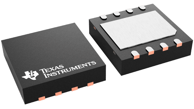
封裝資訊
| 封裝 | 針腳 VSON (DRM) | 8 |
| 操作溫度範圍 (°C) -40 to 140 |
| 包裝數量 | 運送業者 3,000 | LARGE T&R |
UCC27282 的特色
- Drives two N-channel MOSFETs in high-side low-side configuration
- 5-V typical under voltage lockout
- Input interlock
- Enable/disable functionality in DRC package
- 16-ns typical propagation delay
- 12-ns rise, 10-ns fall time with 1.8-nF load
- 1-ns typical delay matching
- Absolute Maximum Negative Voltage Handling on Inputs (–5 V)
- Absolute Maximum Negative Voltage Handling on HS (–14 V)
- ±3-A peak output current
- Absolute maximum boot voltage 120 V
- Low current (7-µA) consumption when disabled
- Integrated bootstrap diode
- Specified from –40°C to 140°C junction temperature
UCC27282 的說明
The UCC27282 is a robust N-channel MOSFET driver with a maximum switch node (HS) voltage rating of 100 V. It allows for two N-channel MOSFETs to be controlled in half-bridge or synchronous buck configuration based topologies. Its 3-A peak source and sink current along with low pull-up and pull-down resistance allows the UCC27282 to drive large power MOSFETs with minimum switching losses during the transition of the MOSFET Miller plateau. Since the inputs are independent of the supply voltage, UCC27282 can be used in conjunction with both analog and digital controllers.
The input pins as well as the HS pin are able to tolerate significant negative voltage, which improves system robustness. Input interlock further improves robustness and system reliability in high noise applications. The enable and disable functionality provides additional system flexibility by reducing power consumption by the driver and responds to fault events within the system. 5-V UVLO allows systems to operate at lower bias voltages, which is necessary in many high frequency applications and improves system efficiency in certain operating modes. Small propagation delay and delay matching specifications minimize the dead-time requirement which further improves efficiency.
Under voltage lockout (UVLO) is provided for both the high-side and low-side driver stages forcing the outputs low if the VDD voltage is below the specified threshold. An integrated bootstrap diode eliminates the need for an external discrete diode in many applications, which saves board space and reduces system cost. UCC27282 is offered in a small package enabling high density designs.
