SLVA959B November 2018 – October 2021 DRV10866 , DRV10963 , DRV10964 , DRV10970 , DRV10974 , DRV10975 , DRV10983 , DRV10983-Q1 , DRV10987 , DRV11873 , DRV3205-Q1 , DRV3220-Q1 , DRV3245E-Q1 , DRV3245Q-Q1 , DRV8301 , DRV8302 , DRV8303 , DRV8304 , DRV8305 , DRV8305-Q1 , DRV8306 , DRV8307 , DRV8308 , DRV8312 , DRV8313 , DRV8320 , DRV8320R , DRV8323 , DRV8323R , DRV8332 , DRV8343-Q1 , DRV8350 , DRV8350R , DRV8353 , DRV8353R , DRV8412 , DRV8701 , DRV8702-Q1 , DRV8702D-Q1 , DRV8703-Q1 , DRV8703D-Q1 , DRV8704 , DRV8711 , DRV8800 , DRV8801 , DRV8801-Q1 , DRV8801A-Q1 , DRV8802 , DRV8802-Q1 , DRV8803 , DRV8804 , DRV8805 , DRV8806 , DRV8811 , DRV8812 , DRV8813 , DRV8814 , DRV8816 , DRV8818 , DRV8821 , DRV8823 , DRV8823-Q1 , DRV8824 , DRV8824-Q1 , DRV8825 , DRV8828 , DRV8829 , DRV8830 , DRV8832 , DRV8832-Q1 , DRV8833 , DRV8833C , DRV8834 , DRV8835 , DRV8836 , DRV8837 , DRV8837C , DRV8838 , DRV8839 , DRV8840 , DRV8841 , DRV8842 , DRV8843 , DRV8844 , DRV8846 , DRV8847 , DRV8848 , DRV8850 , DRV8860 , DRV8870 , DRV8871 , DRV8871-Q1 , DRV8872 , DRV8872-Q1 , DRV8873-Q1 , DRV8880 , DRV8881 , DRV8884 , DRV8885 , DRV8886 , DRV8886AT , DRV8889-Q1
6.3.1 Switch Node
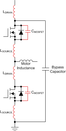
The switch-node is the connection between the source pin of the high-side MOSFET and drain pin of the low-side MOSFET as shown in Figure 6-10. This node is the net that is ultimately connected to the load, which is a motor in this application. The switch node is the most critical signal to be routed in the half-bridge configuration because the high-frequency, high-current nature of the signal on this net. The circuit shown in Figure 6-8 has many non-ideal parasitics caused by the PCB and the power MOSFETs. Figure 6-9 shows a few of these primary parasitics which are the primary causes of a phenomenon called switch-node ringing.
 Figure 6-9 Half-Bridge Parasitics
Switch-node ringing is an LC oscillation on the switch-node due to the parasitics of the PCB and power MOSFETs. Switch-node ringing causes EMI and creates overshoot and undershoot voltages which can violate the absolute maximum ratings of the MOSFET drain-to-source voltage and the gate driver pins. It also can decrease the efficiency of the power stage.
Methods are available to address switch-node ringing through the external measures and system adjustments (reducing slew rates, external snubbers, and others) but a fundamentally sound layout can address many of these primary issues. The layout example in Figure 6-10 shows a design that minimizes the inductance between the source of the high-side MOSFET and drain of the low-side MOSFET. Best practice is to minimize the length and maximize the width of the copper plane connection and using MOSFET packages with minimum parasitic inductance.
 Figure 6-10 Switch-Node Layout Example