SLVA959B November 2018 – October 2021 DRV10866 , DRV10963 , DRV10964 , DRV10970 , DRV10974 , DRV10975 , DRV10983 , DRV10983-Q1 , DRV10987 , DRV11873 , DRV3205-Q1 , DRV3220-Q1 , DRV3245E-Q1 , DRV3245Q-Q1 , DRV8301 , DRV8302 , DRV8303 , DRV8304 , DRV8305 , DRV8305-Q1 , DRV8306 , DRV8307 , DRV8308 , DRV8312 , DRV8313 , DRV8320 , DRV8320R , DRV8323 , DRV8323R , DRV8332 , DRV8343-Q1 , DRV8350 , DRV8350R , DRV8353 , DRV8353R , DRV8412 , DRV8701 , DRV8702-Q1 , DRV8702D-Q1 , DRV8703-Q1 , DRV8703D-Q1 , DRV8704 , DRV8711 , DRV8800 , DRV8801 , DRV8801-Q1 , DRV8801A-Q1 , DRV8802 , DRV8802-Q1 , DRV8803 , DRV8804 , DRV8805 , DRV8806 , DRV8811 , DRV8812 , DRV8813 , DRV8814 , DRV8816 , DRV8818 , DRV8821 , DRV8823 , DRV8823-Q1 , DRV8824 , DRV8824-Q1 , DRV8825 , DRV8828 , DRV8829 , DRV8830 , DRV8832 , DRV8832-Q1 , DRV8833 , DRV8833C , DRV8834 , DRV8835 , DRV8836 , DRV8837 , DRV8837C , DRV8838 , DRV8839 , DRV8840 , DRV8841 , DRV8842 , DRV8843 , DRV8844 , DRV8846 , DRV8847 , DRV8848 , DRV8850 , DRV8860 , DRV8870 , DRV8871 , DRV8871-Q1 , DRV8872 , DRV8872-Q1 , DRV8873-Q1 , DRV8880 , DRV8881 , DRV8884 , DRV8885 , DRV8886 , DRV8886AT , DRV8889-Q1
5.3.1 Near Power Supply
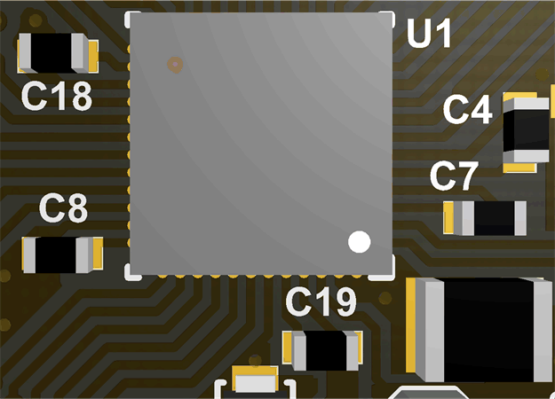
A bypass capacitor is used to minimize high frequency noise into the supply pin of the DRV device. TI recommends placing capacitors as close as possible to the power input pins of the device and ground pins. If the trace lengths between the bypass capacitor and the device are not minimized, they can be inductive at the high frequencies that the bypass capacitor is meant to filter. The added impedance from trace inductance can cause ringing in the voltage or current at the supply pin which contributes to EMI and affects the performance of digital or analog circuits. A best practice is to place the capacitor with the lesser value as close as possible to the device to minimize the influence of the inductance of the trace. Connect larger-value capacitors after the smaller ones because as the value of the capacitor increases the inductance becomes more negligible.
 Figure 5-4 Decoupling Capacitors Close to Device
As Section 3.2 shows, the more vias used, the lower the impedance. TI highly recommends using multiple vias at the power and ground layers. Placing vias directly on the mounting pads of the capacitor can be an effective way to minimize the routing area and still achieve the current flow routing. Follow these guidelines for bypass capacitors:
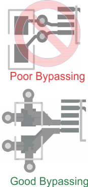
- Do not use vias between the bypass capacitors and the active device. Visualize the high-frequency current flow and reduce loops of high-frequency current as much as possible.
- Make sure bypass capacitors are on the same layer as active components for best results. Do not place a via between the bypass capacitor pin and the IC supply or ground pin.
- Route vias into the bypass capacitors and then into the active component.
- Use the most vias and the widest traces for the best layout.
- The closer the bypass capacitor, the better (less than 0.5 cm, 0.2 in)
- Do not use a length-to-width ratio that is greater than 3:1.
Figure 5-5 shows an example of good and bad bypassing.
 Figure 5-5 Bypass Capacitor Placement