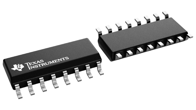
패키징 정보
| 패키지 | 핀 SOIC (D) | 16 |
| 작동 온도 범위(°C) -40 to 125 |
| 패키지 수량 | 캐리어 2,500 | LARGE T&R |
TPL7407LA의 주요 특징
- 600-mA Rated Drain Current (Per Channel)
- CMOS Pin-to-Pin Improvement of 7-channel Darlington Array (For example: ULN2003A)
- Power Efficient (Very low VOL)
- Less Than 4 Times Lower VOL at 100 mA Than Darlington Array
- Very Low Output Leakage < 10 nA Per Channel
- Extended Ambient Temperature Range:
TA = –40°C to +125°C - High-Voltage Outputs 30 V
- Compatible with 1.8-V to 5-V Microcontroller and Logic Interface
- Internal Free-wheeling Diodes for Inductive Kick-back Protection
- Input Pull-down Resistors Allows Tri-stating the Input Driver
- Input RC-Snubber to Eliminate Spurious Operation in Noisy Environment
- Inductive Load Driver Applications
- ESD Protection Exceeds JESD 22
- 2-kV HBM, 500-V CDM
- Available in 16-pin SOIC and TSSOP packages
TPL7407LA에 대한 설명
The TPL7407LA is a high-voltage, high-current NMOS transistor array. This device consists of seven NMOS transistors that feature high-voltage outputs with common-cathode clamp diodes for switching inductive loads. The maximum drain-current rating of a single NMOS channel is 600 mA. New regulation and drive circuitry added to give maximum drive strength across all GPIO ranges (1.8 V–5 V).The transistors can be paralleled for higher current capability.
The TPL7407LA key benefit is its improved power efficiency and lower leakage than a Bipolar Darlington Implementation. With the lower VOL the user is dissipating less than half the power than traditional relay drivers with currents less than 250 mA per channel.
